


fig4
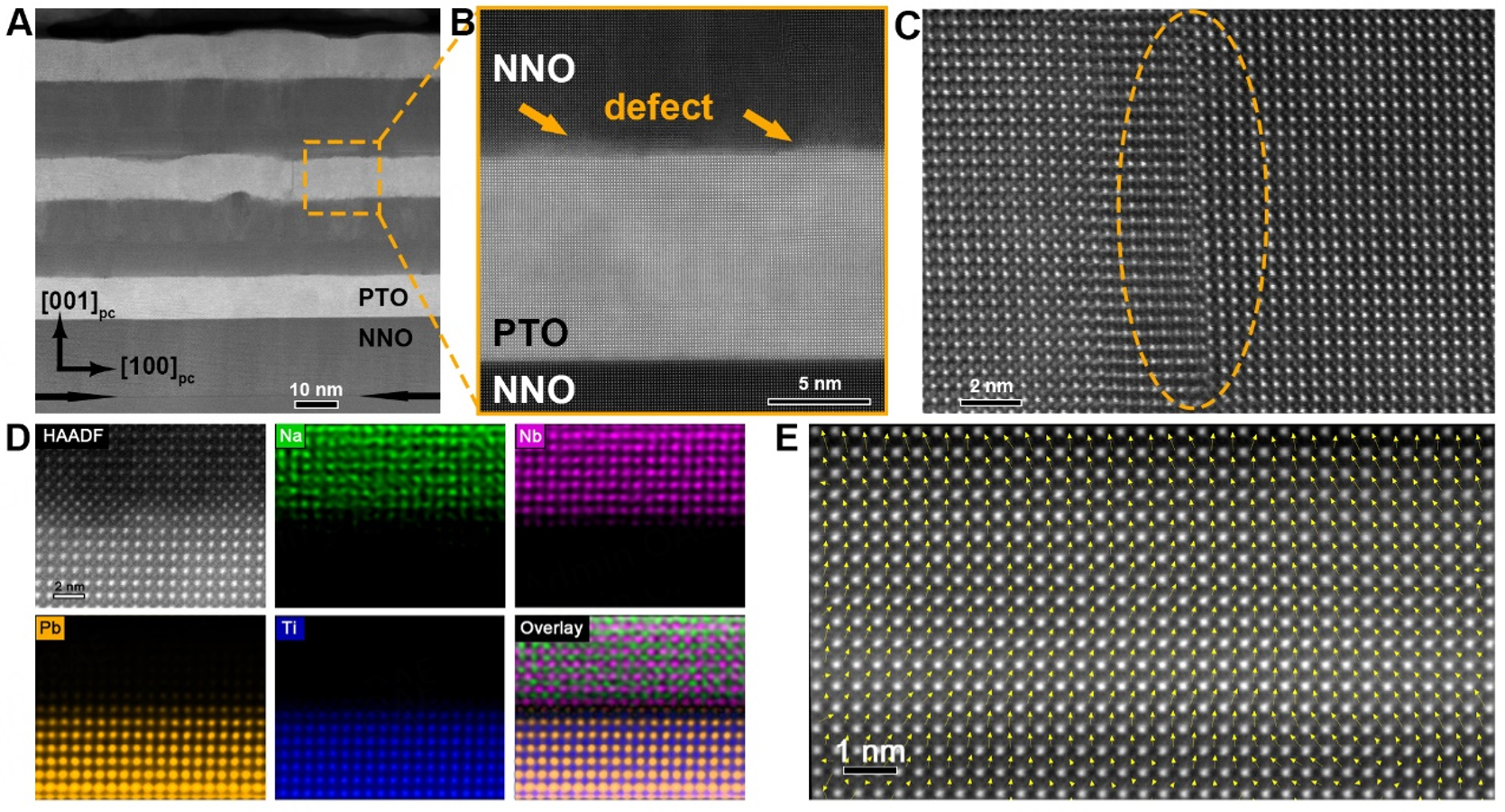
Figure 4. Structure and element analysis of NNO/PTO thin films grown on Nb-STO substrates. (A) Low-magnification HAADF-STEM image of (NNO/PTO)3 thin films and (B) enlarged image of the NNO/PTO interface marked by orange box in (A). (C) Cross-sectional atomically resolved HAADF image of NNO. Antisite NbNa defects can be clearly observed. (D) Atomic HAADF-STEM image and EDS mapping of the NNO/PTO heterointerface. (E) The enlarged atomic positions together with the atomic displacement mapping of Ti ions (yellow arrows) of typical regions near and away from the NNO/BTO interface.


