


fig2
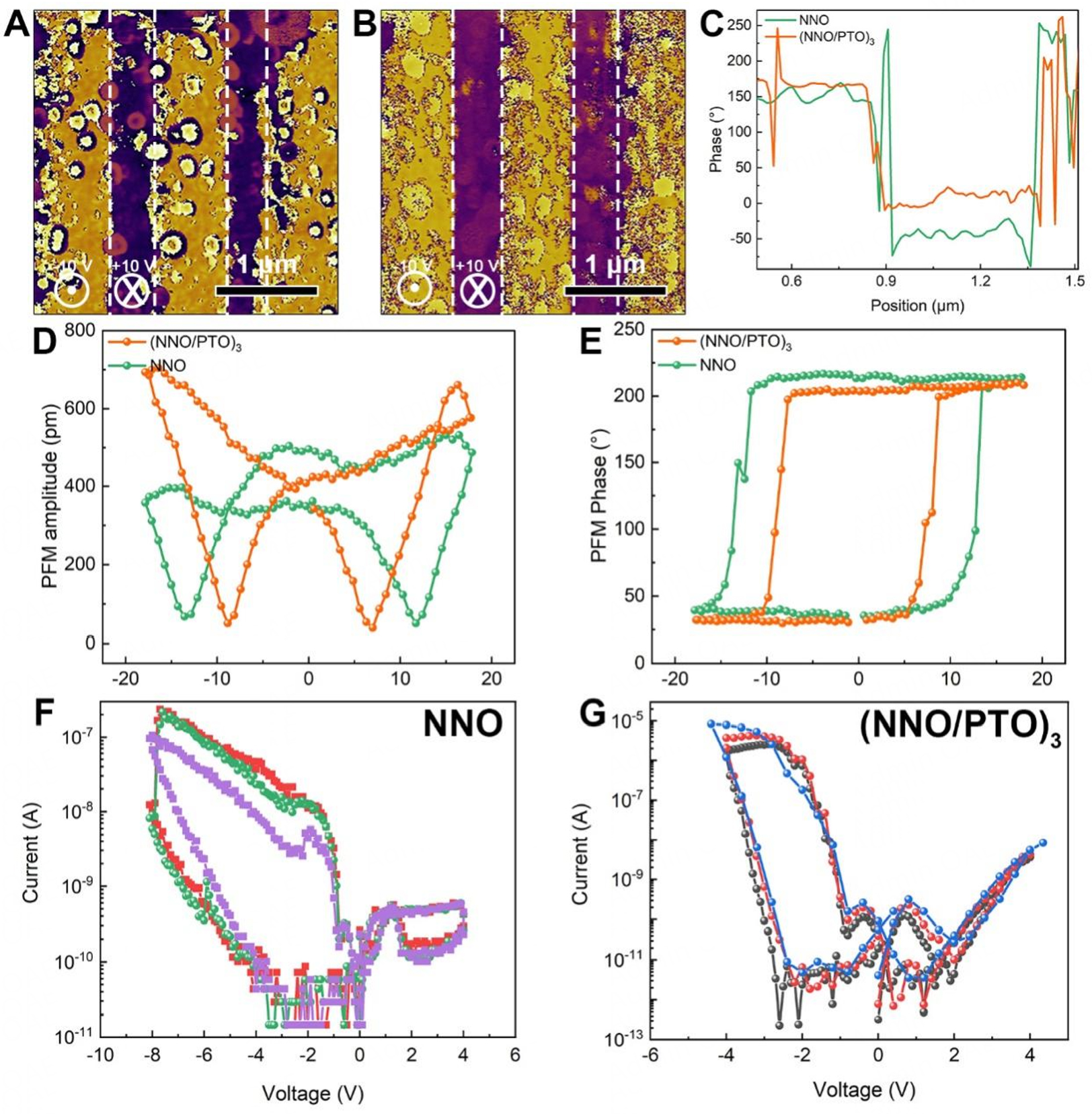
Figure 2. Scanning probe microscopy characterization and nonvolatile resistive switching of Nb-STO/(NNO/PTO)3/Au memristors. (A and B) PFM phase images with square domain patterns written by +10 V and -10 V for NNO and (NNO/PTO)3 film, respectively. (C) Position dependent phase changes along the while lines in (A and B), respectively. (D and E) Amplitude curves (D) and phase switching spectroscopy loops (E) collected with the cantilever for NNO and (NNO/PTO)3 films. (F and G) I-V characteristics for (F) NNO and (G) (NNO/PTO)3 devices.


