


Layer modulating and electrical properties in acceptor-doped Sr5Nb5O17 ceramic with perovskite layer structure


Abstract
Perovskite layer structured (PLS) oxides exhibit some novel physical properties, such as ultrahigh-temperature piezoelectricity, semiconductivity, and oxygen ionic transport. However, synthesizing 5-layer PLS oxides, such as Sr5Nb5O17 ceramics, using traditional solid-state reaction methods is challenging due to their low phase stability. In this study, we propose a new strategy to construct a 5-layer structure from a 4-layer structure. Specifically, Ga-doped Sr5Nb4.444Ga0.556O16.944 (5-SNGO), an iso-structural material to Sr5Nb5O17, was synthesized via a solid-phase reaction. The original design involved co-doping Ga and Mo at the Nb site of the 4-layer parent material Sr2Nb2O7 (4-SNO). However, it was found that only Ga was successfully incorporated into the structure, while Mo remained as SrMoO4, which was subsequently removed by washing with dilute sulfuric acid. X-ray diffraction, transmission electron microscopy, and second-harmonic generation analysis confirmed that the synthesized 5-SNGO ceramic exhibits a 5-layer structure with a noncentrosymmetric space group. The material demonstrated a frequency-independent dielectric permittivity of 60 above 1 kHz. Impedance spectroscopy revealed a very high resistivity of 1.95 × 10⁵ Ω·cm at 900 °C, along with Debye-like dielectric relaxation exhibiting thermal activation behavior. This study presents a novel synthesis approach for constructing 5-layer PLS oxides from a 4-layer structure and provides insights into their structural evolution and electrical properties.

Keywords
INTRODUCTION
As a new type of functional material, layered niobate compounds have attracted much attention for exhibiting special chemical properties in the fields of photocatalysis, ion exchange, high-temperature piezoelectricity, electrochemistry, and photoluminescence[1-6]. The layered niobate compounds belong to the group of perovskite layer structured compounds with the general formula AnBnO3n+2 (A = Sr, Ca, La;

Figure 1. Schematic illustration of crystal structures: (A) 4-layer Sr2Nb2O7 and (B) 5-layer Sr5Nb5O17.
As a multifunctional compound, Sr2Nb2O7 has been extensively studied for its oxygen ion conductivity, dielectric, piezoelectric, and photocatalytic properties, among others[6,12-20]. Notably, Sr2Nb2O7 exhibits high chemical and thermal stability, along with excellent piezoelectric properties and a high Curie temperature (Tc > 1,300 °C). With the in-depth study of oxygen ionic conductors, it has been realized that the introduction of oxygen vacancies through low-valent cation doping is one of the most direct and effective ways for modifying the electrical properties of these materials[21-23]. Previous works have shown that the electrical properties of SrnNbnO3n+2 compounds can be modulated in several ways[24-27]. One approach involves elemental doping or irradiation-induced phase transformation[24,26], while another focuses on modifying the morphology of NbO6 octahedra to achieve the desired electrical properties[25]. However, previous studies have revealed that low-valent single doping at the Sr and Nb sites makes it hard to synthesize a single-phase material and fails to significantly improve its electrical properties[28]. Therefore, co-doping may be an effective way to create oxygen vacancies and investigate their impact on conductivity. In contrast to previous reports, where Sr5Nb5O17 single crystals were typically prepared using the complex floating zone technique while modulating the valence state of Nb through controlled synthesis atmospheres[7], this work introduces equimolar Ga and Mo co-doping to induce oxygen vacancies via a charge compensation mechanism in 4-layered Sr2Nb2O7. This approach successfully yields 5-layered
MATERIALS AND METHODS
Synthesis
Samples of Sr2Nb2-2xGaxMoxO7-0.5x (x ≤ 0.2) were prepared by a conventional solid-phase reaction method with SrCO3 (99.0%), Nb2O5 (99.99%), Ga2O3 (99.99%), and MoO3 (99.90%) as starting materials. After being weighed and repeatedly ground in an alcoholic medium for 2 h, followed by air drying, the well-mixed raw materials were pre-calcined at 1,200 °C for 12 h in the air atmosphere with a heating and cooling rate of
Characterization
X-ray diffraction (XRD) was performed on a Panalytical X’pert Pro X-ray diffractometer with a Cu-Kα radiation source. High-quality laboratory XRD data for Rietveld refinement were collected over a 2θ range from 10° to 80° using an interval of 0.02°. The Pawley and Rietveld refinements of the XRD data were carried out by the Topas-Academic software[29]. The Microstructure and energy disperse spectroscopy (EDS) were performed on a Hitachi (Tokyo, Japan) S4800 scanning electron microscope (SEM). The morphology and internal structure of the prepared samples were further checked by transmission electron microscopy (TEM), selected area electron diffraction (SAED), and high-resolution transmission electron microscopy (HRTEM) using a JEOL JEM-2100F electron microscope operated at a voltage of 200 kV. Elemental mapping of the materials was obtained through an EDAX detector attached to JEOL-2100F. The electrochemical impedance spectroscopy (EIS) was recorded on the Bio-Logic VSP instrument over a 106 to 10-1 Hz frequency range. Both surfaces of the samples were coated with platinum paste and fired at
RESULTS AND DISCUSSION
Phases analysis and purification
X-ray diffraction (XRD) experiments were first performed on the as-made samples from solid-state reaction to investigate the phase compositions for Sr2Nb2-2xGaxMoxO7-0.5x (x = 0.1, 0.2). As shown in
Endeavor to synthesize pure 5-layered Sr5Nb5O17 phase by adjusting the sintering temperature or the proportion of Mo failed, as shown in Supplementary Figure 2 for the products of the sample SNGMO20 prepared under some other conditions. Thus, to get pure 5-layered Sr5Nb5O17 phase samples, a chemical purification method was then applied. For this method, the SNGM20 sample was simply fully washed with dilute sulfuric acid (in which the SrMoO4 was soluble while the niobate insoluble) and followed with liquid-solid separation by filtering three times. The subsequent XRD and TEM/EDX measurements confirmed the pure 5-layered Sr5Nb5O17 phase nature of the yielded dried powders. As shown in Figure 2A and B, all the diffraction peaks in the XRD pattern of the washed sample can be well indexed by the 5-layered Sr5Nb5O17 phase (PDF#83-0603), and no extra peaks from the secondary phase were identified. In addition, obvious segregation of the Mo element was no longer disclosed by the TEM/EDX characterizations on many different areas of the sample, although there was still very weak signal from the Mo element indicating trace concentration in the sample, as shown in Figure 2C for a selected area. Such trace Mo element may originate from the light surface contamination of the insoluble 5-layered Sr5Nb5O17 phase powders with the SrMoO4 solution. Such surface contamination is inevitable and the surface trace SrMoO4 is, therefore, hard to remove completely. Nevertheless, this slight surface contamination was thought to have little, if any, impact on the bulk properties of the 5-layered Sr5Nb5O17 phase sample. Selected area electron diffraction (SAED) further confirmed the 5-layered structure of the purified sample. As demonstrated in Figure 2D, the electron diffraction pattern from the [001] projection direction can be well indexed to the noncentrosymmetric 5-layer structured Sr5Nb5O17 phase with space group Pnn2. The measured interplanar spacings in Figure 2E correspond to the (200) and (010) crystallographic planes of Sr5Nb5O17

Figure 2. (A) XRD patterns of SNGM20 samples before and after washing; (B) Local enlargement of the XRD spectrum in (A); (C) High-angle annular dark field (HAADF) images and energy dispersive spectroscopy (EDS) mapping of SNGM20 powder after washing; SAED (D) and (E) HRTEM images of the SNGM20 powder after washing.
As the Mo element failed in the substitution for Nb and existed in the form of SrMoO4, a more exact composition of the purified 5-layered Sr5Nb5O17 phase sample may be written as Sr1.8Nb1.6Ga0.2O6.1 (viewed as the consequence of subtracting the Mo-containing part of Sr0.2Mo0.2O0.8 from the designed initial composition of Sr2Nb1.6Ga0.2Mo0.2O6.9) and normalized as Sr5Nb4.444Ga0.556O16.944 (or Sr2Nb1.78Ga0.22O6.78). This chemical composition was further supported by the Rietveld refinements for the high-resolution XRD data. For the Rietveld refinements, we used the initial orthorhombic 5-layered Sr5Nb5O17 structure model reported by Schmalle et al. with the space group Pnn2 and containing three Sr sites (two 4c sites and one 2b site), three Nb sites (two 4c sites and one 2a site), and nine oxygen sites[8]. The refinement results revealed that the Ga ions were preferred distributed on the Nb1 site (2a) with an occupancy of about 0.549, with the sum of the occupancy of Nb and Ga constrained to be 1.0 on this site. The other Nb sites and Sr sites are all exclusively occupied by Nb and Sr, respectively, with occupancies close to or even larger than 1.0. For the oxygen sites, although their positions were freely refined, the occupancies of these sites were simply set to be one without being refined, due to their weak scattering power to X-ray. The fitting plots are shown in Figure 3 and the final refined structural parameters are summarized in Supplementary Table 1. The refined cation composition of Sr5Nb0.452(2)Ga0.548(2) further confirmed our above speculation for the actual composition of the purified 5-layer Sr5Nb5O17 phase sample (denoted as 5-SNGO hereafter). However, when we tried to synthesize the Mo-free and Ga-doped Sr2Nb2-yGayO7-y samples, although single-phase products can be obtained for the samples x ≤ 0.15, they crystallized in the 4-layer Sr2Nb2O7 structure, as shown in Supplementary Figure 4.

Figure 3. The Rietveld fitting plots of the SNGM20 powder after washing.
Therefore, it seems that the addition of Mo element is beneficial for the formation of the 5-layer Sr5Nb5O17 phase. In fact, as had been well documented, the crystallized structure type of the SrNbOx system is closely related to the oxygen content x, e.g., SrNbO3.5 and SrNbO3.4 for the 4-layered Sr2Nb2O7 and 5-layered
Defect formation energy calculations
To get a fundamental understanding of the solid solution behavior of Ga doped at the Nb site, defect formation energies were calculated using static lattice atomistic simulations based on the General Utility Lattice Program (GULP)[30,31]. The Buckingham potential function was used to model the interaction between ions with the shell model to describe the electronic polarizability for the structural modeling. The potential parameters used for the atomistic simulation are listed in Table 1 and the well-reproducing experimentally observed crystal structures (see Table 2) validate the feasibility of these interatomic potential parameters.
Potential parameters used for the atomistic simulation
| Interaction | A (eV) | ρ (Å) | C (eV Å6) | k (eV Å-2) | Y (e) |
| Sr2+ - O2 | 1,228.9 | 0.354068 | 0.0 | 34 | 0.74 |
| Nb5+ - O2- | 1,886.3 | 0.332637 | 0.0 | 1,358.58 | 11.097 |
| O2- - O2- | 334,191.667122 | 0.216874 | 701.636798 | 33.909567 | 0.04 |
| Ga3+ - O2- | 1,625.72 | 0.3019 | 0.0 | - | 3.0 |
| Mo6+ - O2- | 797.47721 | 0.435484 | 0.0 | 147.51 | 0.11 |
Calculated and experimental structural parameters for Sr5Nb5O17
| Parameters | Calculated | Experimental | Difference (Calc. - Exp.) |
| a (Å) | 32.4560 | 32.5510 | 0.0950 |
| b (Å) | 5.6740 | 5.5852 | -0.0887 |
| c (Å) | 3.9950 | 3.9313 | -0.0636 |
| Mean Nb1 - O (Å) | 2.0061 | 1.9724 | -0.0336 |
| Mean Nb2 - O (Å) | 2.0143 | 2.0048 | -0.0095 |
| Mean Nb3 - O (Å) | 2.0065 | 1.9981 | -0.0084 |
| Mean Sr1 - O (Å) | 2.4972 | 2.4508 | -0.0463 |
| Mean Sr2 - O (Å) | 2.7349 | 2.6211 | -0.1138 |
| Mean Sr3 - O (Å) | 2.7254 | 2.6339 | -0.0915 |
Then, the energetics of substitutions was calculated for the single Ga doping, as well as the Ga and Mo co-doping on the Nb site, with the creation of oxygen vacancies as charge compensating defects. This doping process of Ga for Nb and Ga/Mo co-doping for Nb can be represented by the following defect reactions (1) and (2), respectively:
The energies of this solid solution reaction can be evaluated by combining the appropriate point defect energy and lattice energy terms. The point defect energies and lattice energies are summarized in Table 3. We can see that the lowest oxygen vacancy formation energy was calculated to occur at the O5 position, suggesting the most likely position for oxygen vacancy. The solid solution energies of Ga substitution for Nb, as well as Ga and Mo co-doping for Nb, in the 5-layered Sr5Nb5O17 structure, are summarized in Table 4, with the oxygen vacancy supposed to be created at the O5 position due to its lowest point defect formation energy as shown in Table 3. The results show that the solid solution energies of Ga doping at the Nb1, Nb2, and Nb3 sites are -15.8931, -1.4693, and -11.6292 eV, respectively, indicating the Ga atoms are preferred to occupy the Nb1 position, which has the highest symmetry among the three Nb sites, and this is in good agreement with the results from Rietveld refinements for the XRD data. In contrast, for Ga and Mo co-doping for Nb1, Nb2 and Nb3 sites, the final calculated solid solution energies are 17.6358, 19.8798, and 18.0536 eV, respectively, which is apparently higher than that of the single Ga doping, which well explains experimentally observed behaviors that the Ga and Mo co-doping failed to obtain single phase and only Ga succeeded in substitution for Nb atoms in the 5-layered Sr5Nb5O17 phase.
Energy of various lattices and defects
| Defect | Energy (eV) | Defect | Energy (eV) |
| 32.70 | Nb2O5 (Z = 14) | -4,742.54 | |
| 32.84 | Ga2O3 (Z = 6) | -925.78 | |
| 34.97 | MoO3 (Z = 8) | -1,675.04 | |
| 22.27 | 62.06 | ||
| 22.23 | 69.27 | ||
| 28.59 | 64.19 | ||
| 23.10 | -36.65 | ||
| 27.36 | -41.62 | ||
| 32.55 | -38.36 |
The extrinsic and intrinsic defect formation energies
| Defect type | Equation | Energy (eV) |
| Acceptor-doping | -15.89 | |
| Acceptor-doping | -1.47 | |
| Acceptor-doping | -11.63 | |
| Acceptor-doping | 17.64 | |
| Acceptor-doping | 19.88 | |
| Acceptor-doping | 18.05 |
Nonlinear optical properties
An optical second harmonic generation (SHG) measurement method was then utilized to investigate the symmetry of the purified sample 5-SNGO. The SHG has a high sensitivity to symmetry breaking and can be used to study the symmetry, ferroelectricity, and ferromagnetism of materials and to determine the phase transition temperature[32,33]. Non-centrosymmetry (NCS) is the prerequisite for an SHG process because the SHG coefficient is zero (χ2 = 0) in all centrosymmetric materials. Therefore, ferroelectric states that do not have inversion symmetry usually provide strong second-harmonic signals, which display second-order nonlinear optical behavior. The SHG plot of the 5-SNGO sample is shown in Figure 4. It can be seen that as the incident light power increases, it needs to pass through a threshold power, which corresponds to the power point where the signal begins to significantly enhance. When the incident optical power squared is greater than 50 mW2, the intensity of the SHG is proportional to the incident light power squared and exhibits second-order nonlinear optical behavior, consistent with the noncentrosymmetric structure with the space group Pnn2.

Figure 4. SHG intensity as a function of the incident light power squared in the 5-SNGO sample.
Ferroelectric measurements
Figure 5A and B shows the ferroelectric hysteresis loops of Sr2Nb2O7 (4-SNO) and 5-SNGO measured at

Figure 5. Polarization-electric field hysteresis loops (P-E) of (A) 4-SNO and (B) 5-SNGO measured at 150 °C, 10 Hz frequency, under different electric fields. Polarization-electric field (P-E) hysteresis loops and charging current density-electric field (I-E) curves for (C)
Dielectric studies
Figure 6 displays the frequency dependence of the dielectric constant (ε′) and dielectric loss (tanδ) for samples 4-SNO and 5-SNGO at room temperature. We can see that as the frequency increases from 102 to ~105 Hz, the dielectric constant decreases sharply (from ~280 to ~90) for the 4-SNO sample, indicating dispersive behavior. Then, the ε′ reaches a constant value at higher frequencies. However, for the 5-SNGO sample, only a slight decrease in ε′ (from ~100 to ~60) was observed within a much more narrow frequency range of 102 to ~103 Hz, and then it kept stable. Usually, for a given sample, the relatively higher values observed at low frequencies may be attributed to the space charge polarization, such as the Maxwell-Wagner effect. The dielectric constant decreases with increasing frequency can be explained by the fact that in a high-frequency electric field, the polarization response could not keep up with the change in the electric field direction, resulting in a decrease in the degree of polarization. For dielectric loss, similar behaviors were also observed that at the low-frequency range, the tanδ of the 5-SNGO sample showed a sharper decrease from 0.60 to 0.006 within the frequency range of 102 to ~105 Hz, while the 4-SNO sample decreased from 0.20 to 0.001 within almost the same frequency range. At higher frequencies, the tanδ kept stable for both samples. The higher dielectric losses at low frequencies are related to the grain boundary defects[34]. Thus, generally speaking, the ε′ and tanδ of the 4-SNO sample are higher than those of the 5-SNGO sample, especially at the low-frequency range, but the 5-SNGO sample displayed better frequency stabilities compared to the 4-SNO sample. Polarization studies show that 5-SNGO has a slightly lower dielectric constant and dielectric loss than 4-SNGO, possibly related to the concentration of oxygen vacancies created by the substitution of Ga for Nb ions. The formation of oxygen vacancies reduces dielectric loss and improves frequency stability. Therefore, the more flattened dielectric constant and lower dielectric loss of the 5-SNGO sample offer better possibilities for applications compared to the classical 4-SNO sample.
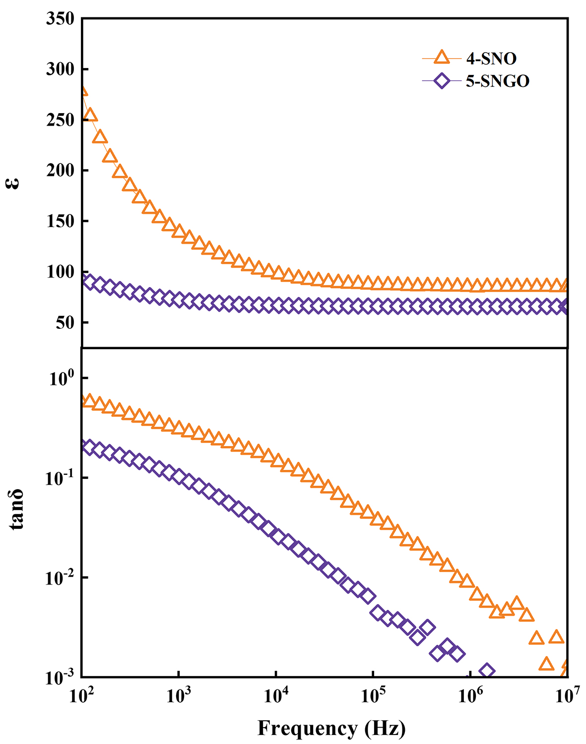
Figure 6. Frequency dependence of the real (ε’) parts of dielectric permittivity and dielectric loss (tan) of 4-SNO and 5-SNGO ceramics at room temperature.
Complex impedance
To investigate the contribution of defective dipole/oxygen vacancies to the electrical properties of 5-SNGO, the complex impedance spectroscopy technique was also applied. Figure 7A shows the complex impedance spectra of the 5-SNGO ceramics, measured over the temperature range of 750 to 900 °C. It can be observed from the figure that only one semicircular arc is observed in the impedance spectrum, which indicates that the ceramic is mainly affected by the grain response and that the resistance of the ceramic decreases with increasing temperature, corresponding to the negative temperature coefficient effect of the ceramic resistor[35], and that the increase in the AC conductivity suggests the thermally activated process of the defective carriers. The DC resistivities of both the 4-SNO and 5-SNGO samples in the range of 600-900 °C are shown in Figure 7B, from which it can be clearly observed that the 5-SNGO ceramic has a resistivity approximately two orders of magnitude higher than that of the 4-SNO, e.g., 1.95 × 10⁵vs. 1.73 × 10³ Ω·cm at

Figure 7. (A) Complex plane impedance plots of 5-SNGO recorded at temperatures 750-900 °C; (B) direct current (DC) resistivity of 4-SNO and 5-SNGO ceramics; (C) frequency dependence of normalized impedance Z″/Z″max of 5-SNGO; (D) the relationship of Z″/Z″max and M″/M″max at 800 °C of 5-SNGO.
where ω0, Ea, kB, and T denote the pre-exponential factor, the relaxation activation energy of imaginary impedance Z″, the Boltzmann constant (8.617 × 10⁻⁵ eV/K), and the Kelvin temperature, respectively. The relaxation activation energy Ea can be obtained from the data points in the plot of ln(ω) versus 1,000/T by linear fitting, as shown in the inset of Figure 7C. The Ea of SNGMO ceramics is 1.79 eV at 750-900 °C.
CONCLUSIONS
In this work, a novel 5-layered Sr5Nb5O17 phase material with the chemical composition of
DECLARATIONS
Authors’ contributions
Sample fabrication and characterization: Duan, X.
Performed the experiments and data analysis: Duan, X.; Xu, J.; Yang, X.; He, X.; Wang, C.
Preparation of the manuscript and discussion: Duan, X.; Xu, J.; Liu, L.
Availability of data and materials
All data and materials included in this study are available from the corresponding authors upon reasonable request.
Financial support and sponsorship
This work was supported by the Guangxi Natural Science Foundation (No. 2021GXNSFFA220002), Science and Technology Plan of Guangxi (No. ZY22096019), National Key R&D Program of China (No. 2022YFF0607805), National Natural Science Foundation of China (Nos. 52172142, 22275057), Innovation Project of Guangxi Graduate Education (No. YCSW2024365).
Conflicts of interest
He, X., from China Nonferrous Metals (Guilin) Geology And Mining Co., Ltd, assisted with second harmonic generation (SHG) measurements using her company's instruments, while the other authors have declared that they have no conflicts of interest.
Ethical approval and consent to participate
Not applicable.
Consent for publication
Not applicable.
Copyright
© The Author(s) 2025.
Supplementary Materials
REFERENCES
1. Ladasiu, C.; Kulischow, N.; Marschall, R. Tuning the photocatalytic activity of layered perovskite niobates by controlled ion exchange and hydration. Catal. Sci. Technol. 2022, 12, 1450-7.
2. Kulischow, N.; Ade, M.; Weiss, M.; Marschall, R. Nitrogen-doped, proton-exchanged Dion-Jacobson layered niobate perovskites for photocatalytic hydrogen generation in solar light. Photochem. Photobiol. Sci. 2022, 21, 1991-2000.
3. Xia, R.; Chen, J.; Liang, R.; Zhou, Z. The positive effect of A-site nonstoichiometry on the electrical properties of Sr2Nb2O7 ceramics for high temperature piezoelectric sensor application. Ceram. Int. 2022, 48, 22459-67.
4. Pan, C.; Zhang, J. C.; Zhang, M.; et al. Trap-controlled mechanoluminescence in Pr3+-activated M2Nb2O7 (M = Sr, Ca) isomorphic perovskites. Opt. Mater. Express. 2018, 8, 1425-34.
5. Kodera, M.; Moriya, Y.; Katayama, M.; Hisatomi, T.; Minegishi, T.; Domen, K. Investigation on nitridation processes of Sr2Nb2O7 and SrNbO3 to SrNbO2N for photoelectrochemical water splitting. Sci. Rep. 2018, 8, 15849.
6. Guo, Y.; Guo, W.; Lei, L.; Xu, J. Oxide ion conduction and transporting mechanism in the layered perovskite-related material
7. Sakai, A.; Kanno, T.; Takahashi, K.; Yamada, Y.; Adachi, H. Large anisotropic thermoelectricity in perovskite related layered structure: SrnNbnO3n+2 (n = 4, 5). J. Appl. Phys. 2010, 108, 103706.
8. Schmalle, H. W.; Williams, T.; Reller, A.; Lichtenberg, F.; Widmer, D.; Bednorz, J. G. A novel semiconducting perovskite-related phase: Sr5Nb5O17. Acta. Cryst. C. Cryst. Struct. Commun. 1995, 51, 1243-6.
9. Kuntscher, C. A.; Schuppler, S.; Haas, P.; et al. Extremely small energy gap in the quasi-one-dimensional conducting chain compound SrNbO3.41. Phys. Rev. Lett. 2002, 89, 236403.
10. Abrahams, S. C.; Schmalle, H. W.; Williams, T.; et al. Centrosymmetric or Noncentrosymmetric? Case study, generalization and structural redetermination of Sr5Nb5O17. Acta. Cryst. B. Struct. Sci. 1998, 54, 399-416.
11. Zhou, Z.; Chen, T.; Liu, X.; Liang, R. Phase transitions and ferroelectricity of perovskite layered Sr2Nb2O7 ceramics. J. Phys. Chem. Solids. 2022, 169, 110888.
12. Song, Y. M.; Dai, J. Q.; Zhang, H. Influence of oxygen vacancy on electric structure and optical properties of pure and N-doped
13. Chen, T.; Liang, R.; Jiang, K.; Hu, Z.; Zhou, Z.; Dong, X. Low-temperature sintering and electrical properties of Sr2Nb2O7 piezoceramics by CuO addition. J. Am. Ceram. Soc. 2017, 100, 2397-401.
14. Cai, X.; Teng, Y.; Wu, L.; Zhang, K. Hot-press sintering Sr2Nb2O7 ceramics and their electrical properties. J. Mater. Sci. Mater. Electron. 2017, 28, 4239-44.
15. Liou, Y. C.; Tsai, W. C.; Yu, J. Y. Effects of La addition on properties of Sr2Nb2O7 thermoelectric ceramics. J. Electron. Mater. 2015, 44, 4857-63.
16. Ojeda-Galván, H. J.; Rodríguez-Aranda, M. D. C.; Rodríguez, Á. G.; et al. Structural and Raman study of the thermoelectric solid solution Sr1.9La0.1Nb2O7. J. Raman. Spectrosc. 2021, 52, 737-49.
17. Chen, G.; Gong, C. W.; Fu, C. L.; et al. Microstructure and dielectric properties of (Ba, Ta) Co-doped Sr2Nb2O7 ceramics. Mater. Sci. Forum. 2015, 815, 125-8.
18. Xiang, L.; Chen, G.; Fu, C.; Cai, W.; Wang, W.; Liu, K. Effect of Ta doping on the microstructure, dielectric and ferroelectric properties of Sr2Nb2O7 ceramics. Ferroelectrics 2014, 467, 165-72.
19. Yuan, Y.; Han, X.; Dong, H.; Zhou, X. First-principles calculation of chalcogen-doped Sr2M2O7 (M=Nb and Ta) for visible light photocatalysis. J. Solid. State. Chem. 2022, 308, 122905.
20. Geng, J.; Chen, Y.; Gu, G.; Tian, L. Tunable white-light-emitting Sr2-xCaxNb2O7:Pr3+ phosphor by adjusting the concentration of Ca2+ ion. Opt. Mater. 2014, 36, 1093-6.
21. Wang, C. M.; Wang, J. F.; Zhang, S.; Shrout, T. R. Piezoelectric and electromechanical properties of ultrahigh temperature CaBi2Nb2O9 ceramics. Phys. Rapid. Res. Lett. 2009, 3, 49-51.
22. Peng, Z.; Chen, L.; Xiang, Y.; Cao, F. Microstructure and electrical properties of lanthanides-doped
23. Gavin, A. L.; Watson, G. W. Defects in orthorhombic LaMnO3 - ionic versus electronic compensation. Phys. Chem. Chem. Phys. 2018, 20, 19257-67.
24. Lichtenberg, F.; Herrnberger, A.; Wiedenmann, K.; Mannhart, J. Synthesis of perovskite-related layered AnBnO3n+2 = ABOX type niobates and titanates and study of their structural, electric and magnetic properties. Prog. Solid. State. Chem. 2001, 29, 1-70.
25. Chen, C.; Yin, D.; Inoue, K.; et al. Atomic-scale origin of the quasi-one-dimensional metallic conductivity in strontium niobates with perovskite-related layered structures. ACS. Nano. 2017, 11, 12519-25.
26. Chen, C.; Wang, Z.; Lichtenberg, F.; Ikuhara, Y.; Bednorz, J. G. Patterning oxide nanopillars at the atomic scale by phase transformation. Nano. Lett. 2015, 15, 6469-74.
27. Chen, C.; Lv, S.; Wang, Z.; et al. Atomic and electronic structure of the SrNbO3/SrNbO3.4 interface. Appl. Phys. Lett. 2014, 105, 221602.
28. Fu, C.; Liu, H.; Chen, G.; Cai, W.; Deng, X. Microstructure and electric properties of strontium lanthanum niobate ceramics. Ferroelectrics 2012, 432, 8-13.
29. Coelho, A. A.; Evans, J.; Evans, I.; Kern, A.; Parsons, S. The TOPAS symbolic computation system. Powder. Diffr. 2011, 26, S22-5.
30. Gale, J. D.; Rohl, A. L. The general utility lattice program (GULP). Mol. Simul. 2003, 29, 291-341.
31. Julian, D. G. GULP: a computer program for the symmetry-adapted simulation of solids. J. Chem. Soc. Faraday. Trans. 1997, 93, 629-37.
32. Ok, K. M.; Chi, E. O.; Halasyamani, P. S. Bulk characterization methods for non-centrosymmetric materials: second-harmonic generation, piezoelectricity, pyroelectricity, and ferroelectricity. Chem. Soc. Rev. 2006, 35, 710-7.
33. Fichera, B. T.; Kogar, A.; Ye, L.; et al. Second harmonic generation as a probe of broken mirror symmetry. arXiv 2019, 1909.12850.
34. Alange, R. C.; Khirade, P. P.; Birajdar, S. D.; Humbe, A. V.; Jadhav, K. M. Structural, magnetic and dielectrical properties of Al-Cr Co-substituted M-type barium hexaferrite nanoparticles. J. Mol. Struct. 2016, 1106, 460-7.
35. Xiong, X.; Tian, R.; Lin, X.; Chu, D.; Li, S. Thermoelectric properties of sol-gel derived lanthanum titanate ceramics. RSC. Adv. 2015, 5, 14735-9.
36. Zheng, X.; Wang, S.; Wang, J.; Hua, W.; Zhang, J.; Liu, L. Long-range and short-range transport dynamics of Li ions in LiMn2O4. J. Phys. Chem. C. 2020, 124, 25254-61.
37. Ang, C.; Yu, Z.; Cross, L. E. Oxygen-vacancy-related low-frequency dielectric relaxation and electrical conduction in Bi:SrTiO3. Phys. Rev. B. 2000, 62, 228.
Cite This Article

How to Cite
Download Citation
Export Citation File:
Type of Import
Tips on Downloading Citation
Citation Manager File Format
Type of Import
Direct Import: When the Direct Import option is selected (the default state), a dialogue box will give you the option to Save or Open the downloaded citation data. Choosing Open will either launch your citation manager or give you a choice of applications with which to use the metadata. The Save option saves the file locally for later use.
Indirect Import: When the Indirect Import option is selected, the metadata is displayed and may be copied and pasted as needed.
About This Article
Copyright


Comments
Comments must be written in English. Spam, offensive content, impersonation, and private information will not be permitted. If any comment is reported and identified as inappropriate content by OAE staff, the comment will be removed without notice. If you have any queries or need any help, please contact us at [email protected].