


Phonon and electron transport engineering for enhanced thermoelectric performance and the challenges of device integration
 0
0 
Abstract
Thermoelectricity has long been recognized as a transformative technology for power generation and cooling, owing to its capability to convert heat directly into electricity and vice versa, thereby facilitating cost-effective and environmentally friendly energy conversion. Following a period of modest activity, the field has experienced a remarkable resurgence since 2000, driven by significant advancements in the development of a diverse array of new materials and compounds, alongside enhanced capabilities for controlled nanostructuring. This rapid growth and the innovative breakthroughs observed over the past two decades can be largely attributed to a deeper understanding of the physical properties at the nanoscale. Among the various thermoelectric materials, nanostructured variants exhibit the highest potential for commercial application due to their unprecedented thermoelectric performance, which arises from substantial reductions in thermal conductivity. However, further advancements will not rely solely on nanostructuring; they will also necessitate novel electronic structure design concepts that require a comprehensive understanding of the complexities of electronic and phonon transport. These developments present significant opportunities for thermoelectric energy harvesting, power generation, and cooling applications. This article aims to summarize and elucidate the breakthroughs reported in recent years, discuss future avenues that integrate nanostructuring concepts with the rich electronic structures of novel materials, and provide a critical overview of the future directions in thermoelectric materials research. Additionally, it offers a comprehensive overview of state-of-the-art thermoelectric materials and devices and a summary of the challenges associated with transitioning these materials into practical devices.

Keywords
INTRODUCTION
Thermoelectric (TE) devices are solid-state systems capable of generating electrical power from heat[1]. They have many advantages over conventional thermomechanical energy conversion devices due to their solid-state nature, absence of moving parts and high reliability. These advantages have led to some noteworthy applications, including the creation of direct electrical power (e.g., power generators for spacecraft), automotive climate control seats, small solid-state cooling diode lasers and infrared sensors, potential applications for power generation from solar irradiation, waste heat recovery, and powering Internet of Things (IoT) devices[2,3]. Companies such as RCA, 3M, Texas Instruments, Marlow Industries, and several other start-ups, have already developed and begun producing TE devices. However, their low efficiency compared to conventional thermomechanical cycles has limited their use to only niche applications and those for which the conventional cycles cannot be easily applied.
The ability of a TE material to convert heat into electricity is quantified by the zT figure of merit, given by zT = S2σT/κ, where σ is the electrical conductivity, S is the Seebeck coefficient (the product S2σ is referred to as the power factor or PF), T is the absolute temperature and κ is the thermal conductivity determining the losses of the process, composed of the electronic and phononic (or lattice) parts as κ = κe + κp. While these transport coefficients of TE materials have been studied for decades, their negative interdependence (σ is inversely proportional to S and directly proportional to κe) has hindered the overall increase in zT[4]. The best commercial materials are based on compounds and alloys of Bi, Te and Pb, and provide zT ~ 1, which corresponds to ~ 10% of the Carnot efficiency[5]. Since Bi2Te3 and PbTe with zT ~ 1 were developed more than 40 years ago [Figure 1], there have been many efforts to increase zT further. Alloy systems and carrier concentration optimization have been investigated as the main drivers to improve conventional thermoelectrics; however, the necessity of optimizing three adversely interdependent parameters in the same material was a fundamental restriction. As a result, around the mid-1970s [Figure 1], optimism faded, basic materials research slowed down, and the mainstream impression in the scientific community was that zT was constrained to unity. For such rather low zT values, the efficiency was insufficient to support competitive products compared to other technologies.

Figure 1. The evolution of the zT figure of merit over decades indicates enormous progress over the last 20 years for many different classes of materials. Data are indicative for the performance of different material families and have been extracted from several Refs.[12-18]. After the initial boost in performance from nanostructuring, the addition of band engineering drives further improvements (regions only roughly denoted).
The resurgence in TE materials research started in the 90s after two influential studies published in 1993 by Hicks and Dresselhaus on Bi nanowires, suggesting an increase in performance from the use of low-dimensional TE materials[6,7]. They essentially provided a paradigm change, pointing out that quantum confinement could offer a fresh approach to improving the efficiency of TE materials. The core premise was that the low-dimensional density of states (DOS) provides sharp features in energy, an element that could largely increase the Seebeck coefficient, independently from the electrical conductivity (i.e., without reducing it), such that large PFs are reached. Although this initial suggestion that quantum confinement will improve the PF was never realized for reasons that we and others explained in later works[8-11], research on nanomaterials quickly led to the realization that nanostructuring offered enormous opportunities for thermal conductivity reductions, from only mild changes all the way to even orders of magnitude. Such works became more frequent in the literature from around the year 2000 onwards, when material synthesis improved to the degree at which adequate control over nanomaterial design was possible. Funding agencies across the globe increased financial support, which led to a resurgence in the field
Data reported in Figure 1 according to their optimal operating temperature range
| Temperature range | Material | Optimal T (K) | zT | Ref. |
| Near Room | Bi2Te3 | 320 | 1.4 | [19,20] |
| AgSbTe2 | 320 | 1.5 | [14] | |
| Iodine-doped Cu2Se | 400 | 2.3 | [21] | |
| Medium | AgSbTe2 | 573 | 2.6 | [14] |
| Zintl phase (Mg3Sb2) | 725 | 1.65 | [15,22] | |
| SnSe polycrystalline | 783 | 3.1 | [12] | |
| InSb | 773 | 1.28 | [15,23] | |
| CoSb3 | 835 | 1.9 | [15,24] | |
| PbTe | 820 | 2.2 | [15,25] | |
| SnSe single crystal | 923 | 2.6 | [18] | |
| High | Cu2-xSe | 1,000 | 1.5 | [15,26] |
| Cu2Se | 1,030 | 2.62 | [15,27] | |
| SiGe | 1,073 | 1.84 | [28] | |
| Half-Heuslers ((Hf,Zr, Ti)CoSb0.8Sn0.2) | 1,073 | 1.0 | [15,29] | |
| Half-Heuslers (FeNbSb) | 1,200 | 1.5 | [15,30] |
Nanostructuring has had such a strong impact on zT through drastic thermal conductivity reductions, allowing zT > 2 across materials and operating temperatures, and dominated the research field in the last 20 years. With thermal conductivities reaching nowadays the amorphous limit and below for many materials, however, further benefits from this approach could be reaching their limits. It is worth mentioning that the reduction of thermal conductivity below the amorphous limit arises mostly from recalibrated models accounting for reduced heat capacity or strong scattering, rather than a fundamental breach of physical limits. For example, porous SiGe nanocrystalline materials reported thermal conductivities of as low as
With the above crucial considerations in mind, this paper describes the main directions for the TE research field over the last period and promising future opportunities. The rest of the paper is organized as follows: Section "REDUCING THERMAL CONDUCTIVITY BY HIERARCHICAL NANOSTRUCTURING" discusses the mechanisms that allowed improvements to zT by nanostructuring, specifically targeting thermal conductivity reductions, and summarizes some of the important milestone works. Section "USING NANOSTRUCTURING TO IMPROVE THE POWER FACTOR" follows with the main approaches to improve the PF of materials, again using nanostructuring and nanomaterials. Section "BAND STRUCTURE ENGINEERING" presents the improvements that band engineering can additionally bring and the promising strategies that are currently followed towards this. Section "TRANSITIONING HIGH zT THERMOELECTRIC MATERIALS TO DEVICES" discusses current state-of-the-art efforts for TE devices: their merits and challenges in practical applications and the main challenges for transitioning from materials to devices. Section "CONCLUSION AND OUTLOOK" finally concludes the review with our wrapping up of the main global considerations on the topic.
REDUCING THERMAL CONDUCTIVITY BY HIERARCHICAL NANOSTRUCTURING
In the context of thermoelectricity, the process and consequence of nanostructuring is essentially to introduce a variety of defects in the channel material to act as phonon scattering centers, reducing the lattice's thermal conductivity. Of course, these also form scattering centers for electrons which reduce the electrical conductivity, but in general, the thermal conductivity is reduced much more since the mean-free-paths (mfps) for scattering of the dominant phonons are in most materials significantly longer compared to those of electrons. The thermal energy-carrying phonons have a distribution of mfps, ranging from nanometers to micrometers, even millimeters. Due to this vast distribution of mfps, one of the most successful strategies to reduce thermal conductivity is to hierarchically nanostructure the materials. This involves the incorporation of a variety of nano-features in the material, each targeting to scatter phonons with different mfps (see Figure 2A). Phonon scattering is characterized by complex dynamics, roughly: (i) atomic-scale defects or alloying that can effectively scatter short wavelength phonons, (ii) nanoscale defects that can scatter short and medium wavelength phonons (with mfps up to ~100 nm), and (iii) micro and mesoscale defects (e.g., grain boundaries) that can scatter long wavelength, low-frequency phonons (with mfps from 100 s of nm to several μm, even up to ~1 mm). Due to their intrinsic size, these nano- and micro-features are also naturally distanced in a hierarchical fashion according to their intrinsic dimension as well, matching the corresponding mfp of the respective targeted phonons, as shown in Figure 2B. Note that the closer these features are placed, the stronger phonon scattering they cause (one could imagine a nanocrystalline material with grains of only several nm). However, this also results in much stronger electron scattering and subsequent PF reduction; electrons are mainly affected by nanoscale defects and their short-range arrangement, with the longer-range defects and arrangements being less relevant. The hierarchical architecture allows taking advantage of the fact that (i) different types of defects target distinct phonons, while (ii) the distance between them is also of the order of those phonon mfps, optimizing strong phonon, but weak electron scattering. In this way, thermal conductivity reduction from phonons across the entire spectrum can be achieved, while the electronic conductivity suffers significantly less[37].

Figure 2. (A) Schematic of hierarchical (panoscopic) nanostructuring, where atomic defects, nanoinclusions, and grain boundaries - spanning atomic to macro scales - act as phonon scattering centers across different mean-free-paths (mfps), reducing lattice thermal conductivity[35]. The lower color plot illustrates typical frequency and mfp contributions to thermal conductivity. Combining various defect types and sizes is essential to target the full phonon spectrum. (B) Nanostructured material schematic showing optimal placement of: (1) Atomistic defects (e.g., vacancies, dopants) for high-frequency phonon scattering, with controlled concentrations to minimize electron scattering; (2) Nanoinclusions of varied sizes and interface types to scatter a wide mfp range while preserving electron transport; and (3) Grain boundaries in nanocrystalline materials for mid- to long-mfp phonon scattering[36], with secondary phases at boundaries to enhance phonon blocking without significantly impeding electron flow.
Although nanostructuring is currently considered the most promising way forward, one needs to consider that some nanofeatures, such as grain boundaries, for example, may suffer from stability and reliability issues. This can be the case if the material is exposed to temperatures higher than those used to produce the material. Thus, to effectively benefit from enhanced phonon scattering along the lifetime of the device/material, it must be operated under conditions at which the nanostructures do not evolve.
One of the earliest and most successful examples of nanostructuring was demonstrated by Biswas et al. for PbTe in 2012, for a system that reached an ultra-low lattice thermal conductivity of κp < 0.9 W·m-1·K-1 at
Such nanostructuring was also able to raise interest for materials that were not traditionally considered good TEs due to their high κp, such as the abundant Si. It was realized early on that Si in the form of nanowires[40-42], superlattices[43,44], porous media[31,45], and combinations of those could result in two orders of magnitude reduction in κp, reaching values close to or even below the amorphous limit. For example, a porous SiGe nanocrystalline material[31] provided scattering of phonons due to alloying, pore scattering and boundary scattering, together with reduced heat capacity because of porosity, which resulted in thermal conductivities of κp = 0.5 Wm-1K-1.
Another highly discussed material is SnSe. Initial reports for the TE performance of the pristine single crystal p-type material indicated a zT value of 2.6[18], sharply peaking at high temperatures due to strong bond anharmonicity, resulting in ultra-low thermal conductivities. This was a new zT record at the time. The corresponding n-type performance reached a zT of 2.2[46]. Many subsequent studies on polycrystalline samples, on the other hand, reported values consistently below unity (although one would have expected that nanostructuring would reduce the thermal conductivity even lower). Later on, another study has, however, treated the samples in a specific way to remove the localized oxygen trapped around the grain boundaries. This resulted in another zT record of 3.1 [see Figure 1][12,33], and better average zT over temperature overall, indicating that the trapped oxygen was hurting the performance in two ways: increasing the thermal conductivity across the grain boundaries, and reducing the electronic conductivity. In other examples, local lattice distortions - such as rattling atoms in skutterudites or strain fields in half-Heuslers - reduce κp by 15%-30% without significantly altering σ[47]. Recent work on Cd-doped-AgSbTe2 nanocomposites demonstrates zT > 2.5 via strain-induced phonon localization, validated by transmission electron microscopy (TEM)[14].
Although initially bottom-up nanostructuring demonstrations were targeted, nowadays top-down approaches, such as mechanical alloying and high-energy ball milling followed by hot pressing sintering or spark plasma sintering (SPS), are widely used to synthesize nanoparticle powders and bulk-size TE materials. This is now widely applied across material families. In this way, the zT values of the different materials were gradually doubled and sometimes even tripled compared to their pristine values. For example, the abundant and non-toxic family of silicides also raised significant interest due to their ability to be nanostructured and extensive studies on these materials exist (Mg2Si[48,49], metal silicides including
Nanostructuring, thus, is a proven strategy that over the past two decades has increased the nominal zT values of the most prominent TEs to the range between 1-2 and sometimes even higher (see Figure 1). There is still some fascinating work to be done to fully understand the effect of nanostructuring on phonon scattering and to create materials that can eliminate most of the phonon contribution to the thermal conductivity (we discuss below an example of a three-dimensional (3D) network material[55] which approaches such point). However, improving the zT further requires improvements to the PF as well, on top of retaining the nanostructured material geometry, for which targeting the roadblock of the adverse interdependence of the electrical conductivity and Seebeck coefficient is encountered. In this regard, directions such as energy filtering and band engineering are shown to be very powerful tools, enabled by developments in the control of nanostructure and alloy synthesis. This was also driven by developments in theoretical and computational tools that enhanced our understanding of transport in complex materials and how chemical bonding affects electronic structure features[13,56].
Importantly, in some of the zT record-breaking works mentioned above, care was taken such that the insertion of nanoinclusions does not degrade the PF significantly. Typically, nanostructuring reduces the electrical conductivity and increases the Seebeck coefficient slightly, but the reduction in conductivity has a stronger influence on the PF[57], which is also reduced, albeit at a smaller degree compared to the thermal conductivity. Some of the ways this PF reduction is mitigated are by aligning the band edges of the constituent material phases such that electronic transport is not noticeably interrupted[17,38,39] alloying using iso-valent substitutions in the lattice (which minimize electron-alloy scattering) using atoms with different atomic weight, like Sr instead of Pb in lead tellurides[17], or Zr and Hf instead of Ti in TiNiSn half-Heusler compounds[58,59]; introducing energy filtering through potential barriers which improve the Seebeck coefficient[57]; through charge transfer from doped islands (modulation doping)[60], or doped interstitial voids[61] in the crystal matrix, which improves conductivity without degrading the mobility, but still reducing the thermal conductivity, etc.
USING NANOSTRUCTURING TO IMPROVE THE POWER FACTOR
Developments in energy filtering
From the above strategies to mitigate the reduction by nanostructuring on the PF, energy filtering is a common underlying cause when PF improvements are encountered. It is typically achieved by the introduction of potential barriers that form at the interfaces between different materials phases, at the grain boundaries and material discontinuities, in the presence of nanoscale defects, etc. These barriers allow high-energy electrons to propagate more easily, while blocking low-energy electrons, thus directly increasing the Seebeck coefficient (see Figure 3). Of course, potential barriers degrade the electrical conductivity. However, design "sweet spots" can be found for which the PF is improved, but even so not significantly, only at the order of 30%[57,62-65]. Nevertheless, a surge in efforts to use energy filtering and design the grain/grain-boundary system efficiently in a variety of materials has recently emerged[66-69].
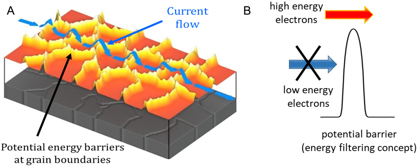
Figure 3. (A) An illustration of the effect of energy filtering at the grain boundaries of a nanocrystalline material. The vertical elevations are a plot of the energy level diagram at the interfaces that the electrons will find, to visually explain the energy filtering process and the potential energy barriers (in yellow) at the grain boundaries, which act as filtering barriers for high-energy electrons. The energy of the current flow (blue arrows) increases locally near the barriers (electrons absorb phonons and gain energy to overpass them) which locally increases the Seebeck coefficient. (B) A schematic of high-energy electrons passing through a grain boundary (potential barrier), where only carriers with energy greater than the barrier height can pass through, while the rest are blocked.
A few experimental designs, however, backed by theoretical calculations, have demonstrated extraordinarily high PFs in Si-based nanocrystalline materials. Specifically, a simultaneous improvement in both the electrical conductivity and the Seebeck coefficient in p-type Si layers was achieved, which led to PF improvements in various instances from 2×-10×[68-73]. For this to be realized, certain design “ingredients” needed to be fit in place: (i) the presence of energy filtering barriers between the nanograins, (ii) the size of the nanograins had to be a few 10 s of nanometers, (iii) ultra-high doping up to the levels of solid solubility had to be used, and finally, and (iv) the materials had to be annealed at high temperatures to allow precipitation of the dopants at the grain boundaries. Compared to bulk Si, whose maximum room temperature PF is approximately ~4-5 mW·m-1·K-2 for p-type and ~5 mW·m-1·K-2 for n-type[74], values of
Theoretical calculations have shown that the properly designed grain/grain-boundary (well/barrier) interface can indeed lead to very high PFs[74]. Such a design includes (i) heavily doped, narrow nanograins that allow access to high carrier energies and velocities, and do not allow significant carrier energy relaxation (to mitigate the local reduction in Seebeck in the grains[64,75]); and (ii) grain-boundaries that provide energy filtering barriers, but themselves and the regions around them are less doped or ‘clean’ from dopants to allow higher carrier mobilities (and mitigate the local reduction in conductivity by the boundaries). Very recently, PF values of ~11 mW·m-1·K-2 were demonstrated in p-type Si that implemented this concept under controlled nanofabrication conditions on a Silicon-on-Insulator (SOI) wafer, a step towards on-chip energy harvesting and cooling[76]. Although this was demonstrated for Si as a flexible platform to control the nano-feature and barrier details[77], this design direction, or parts of it, can widely be applied to other materials as well during the process of nanostructuring.
Developments in 3D nanostructured networks
Even though many nanostructures outperform bulk materials with the same material composition in terms of TE performance, it is crucial to develop structures with nanoscale properties covering wider size scales for use in commercial TE applications. The idea is to combine the advantages of nanostructuring, low-dimensionality, and various interfaces that effectively scatter phonons, into a 3D “size” material. Some of the first examples of this were superlattices, where a periodic arrangement of dissimilar materials creates interfacial scattering and band structure modifications[43,44]. A new direction is the use of proximity field nanopatterning (PnP), a technique that enables the construction of structures with nanoscale feature sizes, while preserving a continuous structure over a sizable region. As an example, a periodic 3D pattern of
Another recent example, which in addition to low thermal conductivity targets high PFs, is a material formed by a 3D nanowire network[55]. A recent study employing 3D/1D anodic alumina templates has demonstrated a remarkable ~5-fold reduction in thermal conductivity in 3D-CuNi nanonetworks. Notably, this significant suppression, relative to the bulk material, has minimal impact on the Seebeck coefficient and electrical conductivity, resulting in an approximately five-fold enhancement in the zT[79]. Similarly, a 3D arrangement of stoichiometric and highly oriented [110] bismuth telluride was created by electrodeposition, consisting of 55 nm diameter longitudinal nanowires joined by 20 nm diameter transversal nanowires. In the longitudinal direction, it was shown that the electrical conductivity of the 3D nanowire network is comparable to the high conductivity typical of Bi2Te3 films produced by the same technique[80]. On the other hand, the Seebeck coefficient increases to values up to
Developments in 2D materials
Monolayers of two-dimensional (2D) materials are emerging as promising candidates for TE materials, offering a novel platform where high electrical conductivity coexists with a high Seebeck coefficient[82,83]. This unique combination is attributed to their low dimensionality, atomically clean surfaces, absence of dangling bonds, and, when prepared with precision, minimal roughness of the 2D surface, which results in reduced quantum well thickness variation. Furthermore, recent studies have uncovered novel phenomena such as metal-insulator transitions[84,85] and electronic correlations that generate charge density waves[86,87], which can enhance TE performance. The ability to create heterostructures also allows for bandgap tuning[88] and renormalization[89], expanding the functional capabilities of these materials.
Recent advancements have indicated the potential for large Berry curvature in stacked 2D materials, which can lead to significant anomalous Nernst coefficients (in the absence of a magnetic field). This property opens avenues for realizing TE spin-Nernst currents, which are particularly relevant for spintronic applications[90-93]. Additionally, 2D materials typically exhibit moderate to low thermal conductivities, especially in the cross-plane direction when monolayers are stacked[82,94,95], which is advantageous for TE efficiency.
The experimental techniques employed to fabricate and investigate the TE characteristics of 2D materials include mechanical exfoliation, which produces single flakes but often results in structural or chemical defects. This straightforward method allows for rapid assessment of TE properties, with promising PFs reported for various 2D materials, such as WSe2, which has demonstrated a PF of approximately
Comparative power factors for Bi2Te3 bulk and various thin films
| Material | Power factor (mW·m-1·K-2) | Temperature (K) | Ref. | |
| Bi2Te3 (bulk) | 4.5 | 300 | [110] | |
| Sb2Te3/MoS2 (multilayer) | 4.9 | 316 | [82] | |
| WSe2 (2D film) | 3.7 | 300 | [96] | |
| NbSe2 (nanosheets) | 0.026 | 300 | [105] | |
| WS2 (nanosheets) | 0.005 | 300 | [105] | |
| Graphene films | 0.6 | 320 | [104] | |
| MoS2 (p-type) | 0.0303 | 460 | [106] | |
| MoTe2 (n-type) | 0.815 | 670 | [107] | |
| Mo-based MXenes | 0.3 | 800 | [109] | |
Alternative approaches, such as intercalation techniques previously applied to non-oxidized graphene, have shown promise in enhancing PFs to over 0.6 mW·m-1·K-2[100-104]. Flexible 2D thermoelectric generators (TEGs) are beginning to emerge in the literature, with examples based on NbSe2 (p-type, PF ~
Thus, 2D materials could have the potential of providing insight into novel physical effects and hold some promise for high performance on par with or even exceeding that of bulk materials[110]. If in the future they overcome challenges related to scalability, stability, etc., they could be at the forefront of the TE technology, particularly in terms of low-power, flexible technologies that enable devices for the IoT and new device concepts to be developed. They will complement the work on films for flexible, room temperature IoT applications, which is also picking up. For this, some promising 2D materials possess the potential to unveil novel physical phenomena and provide high TE performance. The ongoing research in this area is yielding promising results, paving the way for advancements in flexible TE films aimed at room temperature IoT applications[111,112].
BAND STRUCTURE ENGINEERING
Some of the most promising directions for PF improvement in TE materials are summarized by the term “valleytronics”[113]. This involves the utilization of materials with certain features that the valleys in their electronic structure should have, or the engineering of electronic structures to achieve valleys that meet certain criteria. Below we describe these optimal criteria and then some of the efforts undertaken for achieving those through materials engineering strategies. Some examples are shown in Figure 4.
Electronic structure optimal features for TEs
To anticipate at first order if the band structure of a given material will allow for a desirable TE PF, quality factors (or descriptors) have been established. One of the most commonly used is the quality factor,
It has been identified in many studies that for optimal PFs, the Fermi level needs to reside very close to the band edge of the material. In fact, optimal doping is not always achieved in TEs, but it is an important direction that can allow large PF improvements[119]. If a material with its Fermi level placed at its band edge is realized, then many valleys (or transport carrier pockets) would provide increased carrier density and conductivity. Another way to appreciate the importance of the number of valleys, is when examining the material at a fixed carrier density. In this case, a large band degeneracy increases the overall density-of-states effective mass (mDOS) and improves the Seebeck coefficient (the reason being that at a fixed carrier density the Fermi level will be positioned lower if mDOS is higher). On the other hand, a low conductivity effective mass (mC) leads to high carrier mobility and conductivity. The favorable situation will be many light valleys for large mDOS and low mC. An additional important aspect is the degree of inter-valley scattering between these many valleys. This is desired to remain low, because the additional scattering could negate the increase in carrier density and conductivity that large NV brings[120,121]. In many TE materials, the dominant scattering mechanisms are polar optical phonons and ionized impurity scattering (IIS), since TE materials are heavily doped and many are polar. Fortunately, both scattering mechanisms are anisotropic and their strength decays fast with the distance between the valleys in momentum space. Thus, ideally, the optimal TE material electronic structure will consist of: (i) many bands and valleys per band packed closely in energy, (ii) but as further apart as possible in the k-space of the Brillouin zone[118,122] (a definition of Nv as the average number of valleys per band captures some of this[118]), (iii) with light conductivity effective masses, and (iv) large dielectric constant values for enhanced screening and reduction of Coulomb and polar phonon scattering. Such behavior is typically encountered, for example, in most of the materials that exhibit large PFs, such as half-Heusler materials (primarily p-type), chalcogenides, some Zintl phases, silicides, and others. Note that at high carrier densities exceeding 1020 cm-3, screening effects are typically strong and reduce the strength of polar optical phonons. Typically, screening does not become strong enough to do the same for IIS, since IIS also increases with the density of ionized dopants, which is equal to the carrier density. On the other hand, these are anisotropic (small angle) scattering mechanisms, and at elevated densities and Fermi levels, where the Fermi surfaces are large, they only scatter carriers locally in the Brillouin zone, according to the DOS in the vicinity of the initial state, thus not proportionally to the entire DOS. This could make their relative strength reduced compared to non-polar optical phonon scattering, for example, especially at higher temperatures. In other materials such as PbTe with ultra-high dielectric constants, the IIS strength can be diminished, since the scattering strength is inversely proportional to the square of the dielectric constant[123].
Another band structure-related feature that allows for large PFs in complex materials is the presence of complex shaped, elongated energy surfaces in the electronic structure (see Figure 4). Compared to isotropic spherical, or even ellipsoidal bands, elongated, non-parabolic and highly anisotropic features can deliver higher PFs as they can provide simultaneously light effective masses for large electrical conductivity and heavy masses for enhanced Seebeck coefficient. In the limiting case, largely elongated tube-like bands of seemingly lower dimensionality can also provide possibilities for PF improvements and are actively investigated.

Figure 4. Schematics for a few dominant and frequently encountered band structure engineering strategies (clockwise from top): (i) band alignment for increasing the valley degeneracy; (ii) elongated energy surface features; (iii) band inversion followed by spin-orbit-coupling (SOC) for increasing degeneracy and operation close to topological states; (iv) optimal doping; (v) narrow gap materials engineering; (vi) resonant states for Seebeck improvement.
Band alignment materials engineering
For materials with many valleys, but misaligned in energy, significant effort is devoted to properly aligning these valleys using iso-electric alloying (referred to as band alignment or convergence), with very promising results across materials[124]. This is a major band engineering optimization direction currently undertaken (see Figure 4). Many promising examples of materials whose PF benefits upon band alignment can be found in the literature with 10%-50% PF improvements[120]. An effective strategy to achieve band convergence at proper compositions is to use compounds in solid solutions with different band ordering. One example is the solid solution of Mg2X, where X can be Si or Sn. These materials present a conduction band with a dual-band electronic structure (with one heavy and another light band) with an inverted band order for Mg2Si and Mg2Sn. A mixing of the two compounds, around composition Mg2Si0.35Sn0.65, makes the band edges of the light and heavy conduction bands coincide[125]. It is very popular to use solid solutions in thermoelectricity to reduce the lattice thermal conductivity, but equally important is to examine the band structure of the parent compounds and establish opportunities for band convergence. For this, understanding and following the rules of bonding chemistry plays a significant role. For example, in Mn-doped PbTe a smaller energy difference ΔE between the L and Σ pockets is achieved due to the anti-bonding of Te-p and Mn-d orbitals, resulting in the second Σ pocket being pushed upwards[126,127]. Half-Heusler alloys also have multiple pockets in their band structure and are prone to such favorable alloying[30,128]. Moreover, it has been shown that the high TE performance in certain materials is achieved from band convergence with temperature. For example, the high performance of CoSb3 skutterudites arises from the convergence of a secondary conduction band with 12 carrier pockets at high temperatures, rather than from the previously assumed linear band behavior[129]. It is also predicted that the prominent PbTe will also show band alignment of the L and Σ pockets with temperature as well, which will lead to better performance[130] (see Figure 5).

Figure 5. An illustration of the two-valence band (L and Σ) convergence with increasing temperature in certain materials.
Other than forming compounds, band alignment can naturally occur in some multi-band materials at certain temperatures where the different temperature evolutions of the various bands could eventually cause their energy convergence. Materials, such as SnS with three valence band valleys, have temperature dependent valley positions and at certain temperatures alignment can occur which can also reflect on improved PFs[131]. This has also been observed in PbTe and similar rock salt IV-VI compounds and
Band alignment can also be achieved by tuning the material´s structural parameters in certain material families, for example as shown for tetragonal chalcopyrite semiconductors. In cubic zinc-blende compounds, the valence band consists of Γ5V and Γ4V bands, which are split in energy by the crystal field with splitting ΔCF = Γ5V - Γ4V under a non-unity structural parameter η = c/2a[136]. However, it is shown that for
When attempting to reach band alignment, however, details regarding the strength of the inter-valley scattering and the details of the aligned bands need to be considered. For example, theory has shown that in the presence of strong inter-valley scattering, band alignment is only beneficial to the PF when a light mass valley is brought closer to the band extrema to participate in transport (whereas a heavy mass valley can be detrimental). Furthermore, in that case, the bands should not be fully aligned, but an optimal (but small) separation must exist for optimal PF conditions[120]. In the case of weak inter-valley scattering, then any band that is brought into the transport energy window provides PF benefits. Finally, care needs to be taken such that the modifications to the band structure upon band alignment do not alter the masses of the valleys by making them heavier, which will harm the mobility.
Semimetals and narrow bandgap bipolar thermoelectric materials engineering
The bandgap is a crucial component for the TE performance of materials because it creates the necessary anisotropy in the DOS that the Seebeck coefficient requires. TEs require large carrier densities and low effective masses, which are favored by small bandgaps; thus, the interplay between those quantities and some finite bandgap provides some of the best performance TE materials. Lately, however, many reports have appeared in the literature on large PF performance in semimetals or materials with small bandgaps. Most of these cases (that we describe below) have large PFs, but also large thermal conductivities and only moderate zTs (with values not large enough to make it in the plot of Figure 1). Still, high PF materials could be more significant in situations of power generation from abundant heat sources, whereas efficiency could be less important.
A prominent example that has raised significant attention is the full Heusler Fe2VAl. In reference[34], for example, an exceptional PF was reported, originating from a very high Seebeck coefficient, and it is claimed that the n-type Fe2VAl could provide zT even up to 5. This material is claimed to be semi-metallic from ab initio calculations, although a large degree of its behavior can be understood by assuming a small bandgap of 0.02 - 0.04 eV. In fact, with such a small bandgap, due to the large concentration of intrinsic defects (of the order of 1020 cm-3), nominally undoped samples appear metallic[56]. Nevertheless, in Refs.[139,140], it was shown by density functional theory (DFT) calculations that partial Ti or Ta and Si co-substitution in
Another example of how semimetals and/or narrow bandgap materials can provide very high Seebeck coefficients and PFs is when a large degree of anisotropy in transport exists between the conduction and valence bands[118,142,143]. Typically, bipolar transport degrades the Seebeck coefficient which undergoes a zero crossing when the material changes polarity from n-type to p-type when changing the Fermi level position. Furthermore, when the Fermi level is in the bandgap and near the charge neutrality point, where the material is intrinsic (undoped), the carriers experience phonon-limited mobility, which is higher compared to the mobility under heavy doping conditions. In addition, bipolar contributions from both electrons and holes increase the conductivity. Advanced theory and simulations have shown that if quantities such as the DOS, mobility, scattering rates, effective masses, etc., differ significantly between the conduction and valence bands, then the zero crossing of the Seebeck coefficient and the charge neutrality point of high mobility/conductivity occur at different Fermi level positions[143]. This allows for a finite or even high Seebeck at the high conductivity charge neutrality point, and exceptionally high PFs can be realized, even by an order of magnitude higher compared to the unipolar values. Since the electronic thermal conductivity is also large in the bipolar regime, the zT is shown to only increase at most by a factor of 2, which is still significant, while this effect is more evident at higher temperatures[143]. However, in general, bipolar conduction degrades performance and needs to be avoided, because it reduces the Seebeck coefficient and increases the electronic thermal conductivity through conduction of carriers of both polarities, in addition to the bipolar thermal conductivity term (which can be thought as recombination of electrons and holes at the contacts of the material). For example, in narrow-gap materials such as SnSe, bipolar transport degrades the zT at elevated temperatures by introducing such counteracting hole/electron currents[144]. This material-level challenge necessitates bandgap widening via alloying in SnSe, thereby achieving a significant reduction in bipolar conduction[145,146]. Another bandgap engineering direction is related to 2D materials. Theoretical studies have shown that there exists an optimal value for the PF as the bandgap of these materials is reduced as a consequence of the bands becoming more linear, which benefits the electronic conductivity. For even lower bandgaps, however, the PF is reduced because bipolar effects gradually diminish the Seebeck coefficient[147].
Resonant states for Seebeck improvement
Another strategy that led to PF improvements in certain cases is the use of resonant levels which result from interactions between defects and host materials and could lead to an increase in the DOS. This happens in rare cases where certain defects can introduce resonance states and were first observed for Tl defects in PbTe[148]. Typically, the electronic configuration of such dopants is very close to that of the host, as when using periodic table elements from neighboring columns for doping. The goal is to identify a dopant that near the Fermi level forms defect states. The main idea is to increase the DOS locally in energy, such that a broadened delta-function-like feature is added to the underlying DOS of the pristine material. The sharp increase in the DOS is translated into an increase in the Seebeck coefficient, as this coefficient is proportional at first order to the energy derivative of the DOS. As this extra DOS appears at elevated energies into the bands (and assuming that the Fermi level is placed in that vicinity), typically the electronic conductivity does not suffer significantly, or at least PF improvements can be observed. For instance, Tl-doped PbTe exhibits a 3-5× reduction in mobility compared to the single crystal, but shows a 1.7-3× enhancement in the Seebeck coefficient[148], resulting in an overall increase in PF and zT. Since the initial observation[148], a few other cases have been reported. Some other examples are the use of IIIA elements for rock-salt IV-VI structures and functioning as p-type dopants[149-151] and the use of IVA elements in V2VI3 compounds[152]. Additionally, cases such as Sb-doping on the Te-site in CuGaTe2[153], Pb doping on the Bi-site in BiCuSeO[154], and even anti-site defects in ZrNiSn[155], are known for the formation of band edge resonant levels. More lately such effects arising from defect states in Heusler alloys are claimed to provide significant PF improvements[139,140].
Other promising and exploratory directions for PF improvements
Other than the mainstream directions for PF improvements described above, it is worth mentioning exploratory examples based on novel physical phenomena.
One such direction is the increase of band degeneracy in materials with inverted bands in the presence of spin-orbit-coupling (SOC) (see Figure 4). Upon band inversion beyond a critical degree, and under the influence of SOC, a bandgap opens, accompanied by an increase in the number of carrier pockets, the band degeneracy, and as a result it could largely increase the PF. Such effects have for example been predicted recently for rock-salt IV-VI compounds[156,157]. With regards to further utilization of SOC in TEs, recent reports also speculate that the Rashba SOC in 2D materials can modify the DOS distribution and result in lower-dimensional states, which could positively influence the Seebeck coefficient under certain cases[158].
A second exploratory direction is that of topological effects, which have recently emerged with possibly large PF potential. Indeed, a lot of high-performance TE materials are also topological materials. Topological materials have demonstrated a variety of unconventional TE effects that can lead to very high performance. Topological insulators have surface states with almost ballistic conductivity, as backscattering is forbidden by time-reversal symmetry arguments. Although the metallic topological edge states should eliminate S, on the contrary, very large S can be achieved upon SOC induced bandgap opening, further assisted by the low-dimensionality and band linearity[159,160]. This, in addition to the ballistic topological transport (protected from backscattering) which improves σ, could allow for unprecedented PFs. Furthermore, the presence of a non-zero Berry curvature under certain conditions allows the realization of a very large anomalous Nernst effect (ANE), which can also be modulated by gating[90,91,161-163]. These are novel phenomena, but at this point, it is not yet clear if they can provide larger performance compared to the conventional operation. A study on such a Heusler material heterostructure has speculated an incredible
Finally, we need to stress that there are many important developments in materials with important performance features, but not high enough zT to make it into Figure 1, and because of this they sometimes receive less attention. Other than the half-Heuslers mentioned earlier with very high PFs, but zT only around 1-1.5[167,168], we would like to mention the case of Mg3Sb2 and its derivatives[22,169-172]. This material has a zT of ~0.7, but importantly this is at room temperature, which is a range where not many candidates can challenge Bi2Te3. Such a non-Te base material composed of abundant elements can have a much larger impact on room-temperature applications.
Beyond energy conversion and cooling applications, significant interest for TE effects is also encountered in the field of spintronics, where spin currents or voltages need to be created. In particular, the spin-Seebeck effect-SSE (the spin analog of the Seebeck effect), discovered in 2008, has been explored for generation of “spin voltages” driven by thermal gradients (having the ability for spin injection into attached conductors). This gave birth to the field of “spin-caloritronics”. Unlike typical thermoelectrics, which are optimized for highly doped semiconductors, the SSE can be realized in a variety of magnets from - metals to semiconductors and insulators; thus, it could enable insulator-based thermoelectrics[173,174]. SSE was observed in both the transverse configuration, in which a spin current perpendicular to the temperature gradient can be measured, and the longitudinal configuration, in which a spin current flowing in parallel to the temperature gradient is created in the longitudinal direction; thus, this is referred to as the Longitudinal Spin Seebeck Effect (LSSE). The latter has been observed in paramagnetic metal/ferromagnetic insulator junctions, and due to its simplified structure is the mainstream SSE direction[175,176]. However, in this configuration, proximity effects from the ferromagnetic material can result in the creation of the ANE in the metal, in the same direction as the LSSE. Thus, when studying the SSE, separation of the two signals is an important task that is undertaken[177]. Only in magnetic insulators which do not develop the ANE, has the LSSE been measured unequivocally[177]. In general, from the application perspective, the output voltage of LSSE is much smaller than that of conventional devices, but it can be used for spintronic applications, and sensors.
Utilizing the diverse array of materials production and manipulation methods discussed above, a wide range of materials has been explored for TE applications, including Chalcogenides[178,179], Skutterudites[180,181], Zintl phases[182-184], Clathrates[185-187], Full-Heusler[139,188-190], Half-Heusler[191-193], Silicides[194,195], Oxides[196-198], Chalcopyrites[199,200], high-entropy alloys[201,202], transition metal dichalcogenides[203-206], Tetrahedrites[207,208], composites[209-211], and organic materials[212,213], among others[214]. This diverse array of materials encompasses a wide range of structures and properties, aiming to enhance efficiency and performance across different temperature ranges[1,215].
Near-room temperature applications
Bi2Te3 and its alloys have been the benchmark for near-room-temperature TE applications for energy harvesting and cooling[216,217], achieving a zT of ~ 1.4 for Bi2Te3 with various modifications around 300 K[19,20]. However, brittleness, instability under high-temperature gradients, high material costs, and concerns about toxicity, scarcity of the components, and environmental impact, have driven ongoing research into alternative materials. In this sense, Ag2Se has emerged as a more cost-effective and environmentally friendly candidate, achieving near room temperature zT values ~1.2[218-223]. However, the challenge remains to enhance the stability and performance of these materials under operational conditions, particularly regarding thermal cycling, when operating at temperatures above the phase transition, and mechanical stress.
Other TE materials have also been tested for near-room temperature applications. PbTe[224-226],
Medium-temperature applications
For medium-temperature applications, materials such as Skutterudites and Heusler alloys have demonstrated significant potential, with zT values reaching ~ 2. Skutterudites, particularly those based on CoSb3[233,234], have been extensively studied for their ability to achieve high zT values due to their complex crystal structures, which facilitate low thermal conductivity while maintaining good electrical conductivity. Similarly, both half and full Heusler alloys have shown considerable potential in this temperature range, with several compositions yielding zT of ~ 1.5[58,167]. Another well-known material in this temperature range is Mg2Si, which boasts the advantages of being low-cost and non-toxic, showing a zT of approximately 1-1.5 in several studies[235-237].
However, a notable challenge faced by these materials is bipolar conduction, which adversely affects their performance at elevated temperatures. Unlike narrow-bandgap semiconductors or semimetals that excel at lower temperatures, the presence of both holes and electrons in these materials leads to a reduction in the Seebeck coefficient and an increase in thermal conductivity. This interplay ultimately results in a deterioration of the overall zT.
In addition to Skutterudites and Heusler alloys, other materials such as GeTe[238], Cu2Se[239] and PbTe[240] have also demonstrated zT ~ 2 in the medium-temperature range. Among these, SnSe[18,241-244] has garnered significant attention due to its exceptional TE performance, achieving zT values exceeding 3.1 for polycrystalline SnSe[12], underscoring its potential as a simple and cost-effective binary compound with increasing high-performance capabilities. This remarkable performance is attributed to its ultra-low thermal conductivity.
Furthermore, the semiconductor nature of SnSe allows for tunability in both p-type[245,246] and n-type[46,247-249] conduction through the introduction of external dopants, enabling the maintenance of a high zT across different compositions. However, the practical application of SnSe and other selenides is hindered by their sensitivity to degradation, particularly due to the oxidation of Sn, which necessitates extreme purity during synthesis. This sensitivity poses substantial challenges for the scalability and long-term stability of SnSe-based TE devices, which must be, for example, encapsulated. Again, bipolar conduction, prevalent in narrow-bandgap semiconductors, further limits their effectiveness at elevated temperatures, highlighting the need for ongoing research into alternative materials and strategies to mitigate these issues.
High-temperature applications
High-temperature TE materials are essential for applications in remote power stations, deep-space spacecraft exploration powered by radioisotope TEG, etc. Oxides and silicides are predominant in this domain, i.e., metal oxides, including ZnO[250-252] doped with Al[253,254], have been widely studied for such applications. Other oxides such as MgO, Cr/Mo/Ru/MnFe2O4[197], Ba1/3CoO2[255], cobalt-oxide[198], and SrTiO3-based[256] have also garnered attention. There are non-oxidic materials like Cu2Se (which has demonstrated zT of ~2 around 1,000 K[239], while Cu2Se-BiCuSeO-graphene composites have shown exceptional potential, achieving a zT = 2.82 at 1,000 K[257], and Si-Ge[258] alloys have shown promise at high temperatures. However, these materials must endure significant thermal stress, which can induce mechanical failure and maintain chemical instability, which poses a challenge for their long-term performance. Si-Ge alloys have been shown to have long stability and have been used by the National Aeronautics and Space Administration (NASA) in the spacecraft Voyager, Galileo, Ulysses, Cassini, and New Horizons[258,259]. Although theoretical predictions suggest a thermoelectric zT exceeding 2 for Si-Ge systems[260], experimental studies have reached approximately 1.84 at 1,073 K[28].
It is also important to note that at very high temperatures, the strategy of nanostructuring may be compromised, as materials must endure extreme temperatures for extended periods. Table 3 provides a detailed list of the state-of-the-art TE materials and their performance according to their operational temperature.
State-of-the-art TE materials according to optimal temperature and their respective zT
| Temperature range | Materials | Details | zT | Ref. |
| Near room | Bi2Te3 | Bi1.8Sb0.2Te2.7Se0.3+ 15 wt% Te | 1.4 | [19] |
| (Bi2Te3)0.93(Ga2Te5)0.07/Bi1.99Ga0.01Te3 | 1.5/1.2 | [20] | ||
| Bi2Se0.02Te3Cu0.03(Cu2S)0.0125 | 1.6 | [211] | ||
| BiSb0.95Ag0.05Te2Se | 1.7 | [261] | ||
| Ag2Se | Zn-doped β-Ag2Se | 1.3 | [220] | |
| Ag2Se nanorod arrays | 1.15 | [221] | ||
| β-Ag2Se (porous polycrystalline bulk) | 0.9 | [222] | ||
| Ag2Se via PHRMS | 1.2 | [218] | ||
| Mg3Bi2 | Te-doped Mg3Sb2 single crystal | 0.5 | [171] | |
| Mg3.2Bi1.5Sb0.498Te0.002Cu0.01 | 0.9 | [229] | ||
| Mg3Sb2 | Mg3Sb1.48Bi0.48 Te0.04 | 0.6 | [22] | |
| Sb2Te3 | Sb2Te3/MoS2 Multilayer | 2 | [82] | |
| Sb1.97Nb0.03Ag0.005Te3 | 0.6 | [227] | ||
| Sb2Te3 + 15% Bi2Te3 | 1 | [178] | ||
| AgCuTe | (AgCu)0.995Te0.9Se0.1 | 1.1 | [232] | |
| Medium | SnSe | Polycrystalline SnSe | 3.1 | [12] |
| Single crystals along the b-axis | 2.6 | [18] | ||
| Bi-doped SnSe single crystals | 2.2 | [46] | ||
| PbTe | Pb0.98Na0.02Te-8%SrTe | 2.5 | [32] | |
| Pb0.97Na0.03Te-2%MgTe-0.75%GeTe | 2.8 | [224] | ||
| 2.5% K-doped PbTe0.7S0.3 | 2.2 | [240] | ||
| PbSe | Cu0.005PbSe0.99Te0.01 | 1.7 | [61] | |
| Mg3Sb2 | Mg3.1Co0.1Sb1.5Bi0.49Te0.01 | 1.7 | [170] | |
| Mg3Sb1.48Bi0.48 Te0.04 | 1.65 | [22] | ||
| CoSb3 | (Sm,Mm)0.15Co4Sb12 | 2.1 | [262] | |
| CoSb2.875Te0.125 | 1.1 | [233] | ||
| Yb0.35Co4Sb12 | 1.5 | [263] | ||
| GeTe | Bi0.05Ge0.99Te | 2.0 | [238] | |
| ZrCoBi | ZrCoBi0.65Sb0.15Sn0.20 | 1.42 | [167] | |
| (Zr, Hf) NiSn | Ti0.5(Zr0.5Hf0.5)0.5NiSn0.998Sb0.002 | 1.5 | [58] | |
| BiCuSeO | Bi0.94Pb0.06CuSeO | 1.14 | [154] | |
| AgSbTe2 | AgSb0.94Cd0.06Te2 | 2.6 | [14] | |
| Mg2Si | Mg2Si0.785Sn0.2Sb0.015 | 0.95 | [236] | |
| Mg2.03(Si0.3Sn0.7)0.993Bi0.007 | 1.3 | [237] | ||
| Mg2.08Si0.364Sn0.6Sb0.036 | 1.5 | [264] | ||
| High | SiGe | Polycrystalline n-type SiGe alloys | 1.84 | [28] |
| Si80Ge20B0.8(TaC)1 | 1.06 | [258] | ||
| Ba1/3CoO2 | Ba1/3CoO2 epitaxial film | 0.55 | [255] | |
| Yb14MnSb11 | Yb14MnSb11 with 5% excess Mn | 1.2 | [265] | |
| Yb14MnSb11 prepared with MgH2 | 1.26 | [266] | ||
| Cu2Se | Cu2Se - Co-coated B nanoparticles | 2.23 | [267] | |
| Cu2Se-BiCuSeO-graphene | 2.82 | [257] | ||
| FeNbSb | FeNb0.88Hf0.12Sb | 1.5 | [30] | |
| Pr3Te4 | Pr2.74Te4 | 1.7 | [165] | |
| La3Te4 | La2.2Ca0.78Te4 | 1.2 | [268] | |
| SrTiO3 | SrTiO3-10 mol% La-10 mol% Nb | 0.65 | [269] |
TRANSITIONING HIGH zT THERMOELECTRIC MATERIALS TO DEVICES
The landscape of TE materials has evolved significantly over the past few decades due to advancements in phonon and electron transport engineering. While materials with zT > 2 are now commonplace in laboratory settings, their translation into commercially viable TEGs requires addressing critical challenges at the device integration level. This section gathers critical insights to highlight the most significant challenges and considerations in this transition and future priorities.
Scalability and processing challenges: The first major bottleneck is scalability and manufacturing. Current synthesis methods for hierarchical nanostructures (e.g., ball milling, SPS) face limitations in producing homogeneous bulk materials at industrial scales. For instance, while PbTe-SrTe nanocomposites achieve
Materials selection: Another significant factor is the selection of TE materials, which must exhibit optimal TE properties, including a high Seebeck coefficient, electrical conductivity, and low thermal conductivity. While traditional materials such as bismuth telluride (Bi2Te3) and lead telluride (PbTe) have been extensively used, they face limitations at elevated temperatures, necessitating the exploration of alternative materials. Recent studies have highlighted the potential of materials such as germanium telluride (GeTe) and skutterudites, which have shown promising zT values in the medium-temperature range. However, the performance of these materials can be adversely affected by bipolar conduction at higher temperatures, which necessitates ongoing research into alternative compositions and doping strategies to enhance their TE performance.
Innovative methods of doping and structural optimization further augment performance. For example, entropy engineering, Te-capping, doping, etc., in Bi2Te3 has significantly reduced tellurium sublimation losses, contributing to minimal zT degradation after extensive testing[274-276]. The exploration of materials such as Ag2Se, PbSe, GeTe and Sb2Te3, in conjunction with state-of-the-art skutterudites and Heusler alloys, indicates the move towards developing high-performance TE materials for various applications[219,227,238,277].
Interface engineering and diffusion barriers: Another important bottleneck in enhancing device performance and stability lies within the interfaces between TE materials and electrodes. A primary challenge is preventing interdiffusion, which can lead to the formation of undesirable phases and subsequent performance degradation. Each interface must be tailored to the specific TE material to ensure optimal efficiency and reliability. Notably, interfaces within multilayered segmented TE legs necessitate extensive characterization and optimization to leverage high-performance materials such as Bi2Te3, PbTe, and Mg3Sb2, among others, that have shown significant zT values[278,279]. These interfaces critically influence thermal and electrical contact resistance, directly affecting overall device efficiency. Therefore, strategies to mitigate interdiffusion and minimize electrical resistance while minimizing thermal losses are essential for improving device TE performance[280].
Innovative interface engineering techniques have been utilized to address interdiffusion challenges. The application of diffusion barrier materials, such as Ni-P coatings or TiN/Mo in PbTe-based and Bi2Te3-based TE modules, has effectively prevented detrimental interdiffusion with solder materials, while also enhancing bonding strength and resistance to intermetallic formation, ensuring greater reliability at elevated temperatures[278]. Further, Co-P diffusion barriers have been employed to stabilize joints in PbTe TE materials, significantly reducing atomic interdiffusion and prolonging the device lifespan at high operational temperatures[281]. Additionally, titanium layers have demonstrated improved interfacial stability against copper diffusion in Bi2Te3, maintaining low contact resistivity and notable mechanical strength[282].
Moreover, recent advancements have explored novel barrier materials like Mg2Ni, which prove compatible with TE phases such as Mg3Sb2[280]. This approach minimizes interfacial stresses, thereby enhancing overall device performance[280,283]. Furthermore, ongoing research into metal-semiconductor interfaces continues to present promising avenues for optimizing TE efficiency.
Soldering and bounding process: Soldering and bonding processes used to connect TE materials to electrodes also present critical challenges. Traditional soldering materials may not provide adequate thermal and electrical conductivity; thus, the exploration of new soldering materials is essential to improve performance. The impact of soldering processes on the microstructure, including crystal orientation and grain boundaries, must be thoroughly assessed to understand how these factors influence the TE properties of assembled devices. Traditional Sn-based soldering materials often exhibit limited temperature stability. In contrast, Ag-based bonding materials serve as a viable alternative, utilized in both micron-sized flakes and nanoscale paste forms, yet they do carry cost and environmental concerns[284]. Recent developments of transient liquid phase bonding[285] offer low-temperature solutions while maintaining high-temperature stability, alleviating the detrimental effects of thermal damage on the TE material and interface.
Operational degradation: The operational degradation of TE materials constitutes an additional challenge, driven by mechanisms such as elemental diffusion, self-diffusion, and thermal stresses[286]. Critical design considerations, including encapsulation techniques, have emerged as effective strategies for mitigating these degradation mechanisms. Encapsulation protects TE materials from environmental factors, such as oxidation, which can undermine their stability at high temperatures. For example, encapsulation strategies in Ag2Se-based flexible devices have been demonstrated to prevent the propagation of microcracks, significantly enhancing mechanical flexibility while maintaining performance integrity even after 2,000 bending cycles[287]. Moreover, to mitigate surface-related degradation and ensure long-term stability - such as oxidation and magnesium loss in Mg3Bi2-based systems - coating or encapsulation with chemically inert materials such as BN, MgO, and SiC has proven to be an effective approach[288]. Furthermore, advanced techniques, such as Mg-vapor annealing, bolster thermal stability by preventing adverse phase transitions[288, 289]. In similar vein, Sulfur infusion is reported to enhance both TE performance and stability of sulfides[290]. The application of Al2O3 atomic-layer-deposited coatings of 50 nm for on semiconducting single-walled carbon nanotube has demonstrated impressive retention of 95% of conductivity and PF after 300 h in air, underscoring the need of encapsulating materials to enhance TE resilience[291].
Material degradation: The degradation of TE materials during operation is another critical challenge. Several mechanisms contribute to this degradation, including elemental diffusion and self-diffusion within the TE materials and contacts, sublimation of dopants, moisture-induced degradation, structural defects accumulation, thermal stresses, chemical interactions with other materials in the TE system and the formation of intermetallic compounds. These can compromise the mechanical integrity and TE performance of the modules over time[292,293]. Furthermore, the coefficients of thermal expansion (CTE) of different materials in a TEG must be carefully matched to prevent mechanical stresses during thermal cycling. Mismatches can lead to cracking and delamination at the interfaces, significantly affecting the durability and performance of the device[294]. The design of the module must account for these differences to ensure long-term stability under operational conditions. Such considerations also hold true for high-performing Ag/Cu/Sn-based selenides, which exhibit excellent TE performance, but undergo several phase transitions at elevated temperatures. Sublimation of Se and the need to use an extremely pure environment to prevent oxidation are critically important to maintaining the high performance of these materials[12].
Mechanical stability: The mechanical stability and reliability of TEGs under varying thermal and mechanical loads is a significant concern. The design must ensure that the modules can withstand harsh environments and repeated thermal cycling without failure. This requires a thorough understanding of the mechanical properties of the materials and the effects of thermal stress on the interfaces. Operational control mechanisms are essential for maintaining consistent performance in TEGs. Effective temperature regulation requires advanced control systems that can monitor and adjust operational parameters, such as temperature and electrical output. The integration of power management systems is also vital to ensure compatibility with external loads, which adds complexity to the overall system design.
Integration with modern electronics: The solid-state nature and versatility in size and shape of TE make them suitable candidates for integration into modern electronics and sensors[279,287], as well as integration with other systems such as photovoltaic[295], wearables[296,297], and power electronics[298], etc. For integration with power electronics and other applications, modern TEGs require co-design with wide-bandgap semiconductors (SiC, GaN) to handle maximum power point tracking (MPPT) at > 90% efficiency[299-301]. Moreover, heterogeneous integration using ultra-deep through-silicon vias (TSVs) reduces parasitic resistance in Si-based devices[302].
Finally, the performance testing and its optimization is something that must also be researched to be able to transition from high zT materials to high ZT devices. The performance of TEG modules must be rigorously tested under various conditions to ensure reliability and efficiency. This includes evaluating their performance, along with other parameters such as internal resistance, and overall stability of the modules under different atmospheric conditions and temperature cycles. While significant advancements have been made in the development of TE materials, each category presents specific challenges that must be addressed to facilitate their transition into the market. Ongoing research is essential to optimize these materials for stability, performance, and cost-effectiveness, ensuring their viability for commercial application.
Several examples of the transformation from materials to functioning TE devices - with increasing overall device efficiency and their key limitations - have been reported in the literature, as discussed in Table 4. Various materials such as Mg3Sb2[309], GeTe[311], and half-Heusler[318] phase compounds-based TE modules have demonstrated efficiencies exceeding 10% across diverse temperature gradients, which is higher than commercially available Bi2Te3-based modules. For example, NASA has been employing SiGe- and PbTe-based TE modules in various space exploration missions, with an efficiency of 6.3% at a temperature gradient of 700 K and 328 K for SiGe- and PbTe-based systems, respectively[323].
State-of-the-art thermoelectric module efficiencies (η) across various temperature gradients (ΔT) and their associated limitations
| Material | η (%) | ΔT (K) | Key limitations | Ref |
| Bi2Te3 | 8 | 230 | Bi2Te3 modules suffer from Te scarcity (€1100/kg) and degradation above 250°C | [80,303-305] |
| PbTe (Apollo mission) | 6.3 | 328 | High-cost; Both elements are toxic; limited temperature stability; Interfacial reactions | [306,307] |
| GeTe-Mg3SbBi | 10 | 350 | High materials cost (Ge/Te); toxicity (Te/Sb); Other considerations for MgSb- and GeTe-based systems as discussed below | [308] |
| Mg3Sb2-single leg | 10 | 350 | Stability issue at higher temperatures; Mg sublimates above 450°C, requiring encapsulation | [309] |
| GeTe-Cu2Te-PbSe- single leg | 14 | 440 | High Cost of Ge (€3500/Kg according to Aldrich webpage) and toxicity concerns (Ge/Pb/Te); Phase transitions at elevated temperatures | [310] |
| GeTe-based | 13.3 | 506 | Expensive; Te-toxicity; Diffusion of materials and electrodes; Service reliability concerns, as the secondary phases are observed | [311] |
| Ge0.89Cu0.06Sb0.08Te-Yb0.3Co4Sb12 | 12 | 545 | Aging ingresses the interface resistivity. Phase transition in GeTe at elevated temperature | [312] |
| Mg3Sb2-MgAgSb | 7.3 | 593 (hot side) | Brittleness; Oxidization and moisture sensitivity; Bipolar effect | [313,314] |
| PbTe-Bi2Te3 cascaded module | 12 | 590 | Deterioration of the interfaces between the legs and electrodes; toxic and high-cost material | [315] |
| (Nb0.8Ta0.2)0.8Ti0.2FeSb -Hf0.5Zr0.5NiSn0.98Sb0.02 | 8.3 | 655 | Challenges in scaling up homogeneous materials for large-scale applications; dopant Ta hard to melt and diffuse. | [316,317] |
| (Nb, Ta, Ti, V) FeSb | 15.2 | 670 | Significant efficiency drops at lower temperature; Though stable contacts long term stability concerns. | [318,319] |
| SiGe (Voyager mission) | 6.3 | 700 | Low efficiency; Increasing cost of Ge; Prone to microcracks and mechanical failures; Interdiffusion of electrodes | [306,320-322] |
Lastly, it is vital to consider the market positioning of TE modules in relation to competing technologies. From an energy generation perspective, alternatives such as internal combustion engines (ICEs), organic Rankine cycle (ORC) systems, photovoltaics (PV), fuel cells, and piezoelectric or triboelectric generators pose significant competition. For refrigeration applications, vapor compression systems (VCS), magnetocaloric refrigeration (MCR), phase-change materials, and microfluidic cooling are key rivals. Currently available TE systems, which exhibit an efficiency of around ~10% as generators and a coefficient of performance (COP) of less than 1 as coolers, offer lower performance compared to ICEs, PV, and fuel cells. The same is true when compared to VCS and MCR. However, their solid-state nature, reliability, low maintenance, and size versatility make them viable for a wide range - from large-scale systems to microelectronic devices, including various autonomous and sensor applications. In a similar vein, cooling using thermoelectric coolers (TECs) offers higher precision and control, and their compact nature enables easy and scalable integration. In fact, integration of thermoelectrics with other sustainable solutions such as PV and ICEs has shown improvement in the overall system efficiency. It is also important to note that TEGs outperform piezoelectric and triboelectric generators, and TECs can be an effective cooling solution for microelectronics. It is worth mentioning that while TEGs excel in niche applications - such as wearables[296], space power[306] - they face stiff competition from ORCs in waste heat recovery scenarios. Techno-economic analyses indicate that TEGs become commercially viable at heat fluxes exceeding 5 W·cm-2, where ORC systems struggle due to high maintenance costs[324]. Recent advances include the demonstration of a 600 W TEG prototype integrated into a BMW X6, highlighting progress toward the U.S. Department of Energy’s $1/W cost target[325,326] for automotive applications. In parallel, material innovations such as Cu/Ag co-doping in bismuth telluride alloys have been shown in laboratory studies to reduce tellurium content by up to 40%, potentially contributing to future cost reductions, while also working on element recovery after the car is not more in use. One promising solution lies in circular economy approaches, such as the electrochemical recovery of critical elements like copper, bismuth, tellurium, and antimony commonly used in TE modules[327,328].
Therefore, the broader adoption of thermoelectric modules depends on a holistic approach that advances materials development and improves device integration, as discussed in detail above, while simultaneously addressing both cost-effectiveness, environmental sustainability and recyclability.
CONCLUSION AND OUTLOOK
In this paper, we have reviewed the progress of the thermoelectric research field and discussed the most promising future directions. We focused mainly on novel concepts that have been introduced over the years, which have allowed for the remarkable progress experienced. Over the last 20 years, the resurgence in thermoelectric research and the advances in the zT are attributed significantly to nanostructuring and the large reduction in the thermal conductivity that accompanies it. Advanced nanostructuring methods have been developed, in which defects are introduced in a pristine material at the atomic-, nano-, and macro-scale, scattering phonons of different mean-free paths and reducing the thermal conductivity across the phonon spectrum. zTs have more than doubled to values of zT ~ 2, not only for the traditional thermoelectric materials, but for many more material families, which entered the field due to this drastic reduction in thermal conductivity. Some of the best results were reached when care was taken not to reduce the electronic conductivity significantly, for example, by using iso-electronic doping/alloying and nano inclusions whose band edges are aligned with the matrix material. Nanostructuring can also offer significant advantages to the power factor as well, utilizing the concept of energy filtering, which allowed unprecedented PF values in some cases that followed specific design guidelines. An even higher boost in the zT is on its way by utilizing band structure engineering techniques to improve the PF further. The most studied method is the so-called band alignment (or band-convergence) in which multi-band electronic structures undergo specific alloying such that many bands are aligned in energy and all contribute to transport. Many other concepts are explored, such as resonant states, topological effects, defect engineering, and transport in low bandgap materials and/or semimetals. The exploration of these newly emerged physics-based concepts and their integration into different materials is only the starting point, and many exciting outcomes are expected in the future in the field of thermoelectrics.
However, the transition from thermoelectric materials to TEG devices presents its own set of challenges that must be addressed for successful commercialization of these materials with high efficiency. Key issues include interface engineering, where the complexity of interfaces between different TE materials can lead to increased thermal and electrical contact resistance, negatively impacting efficiency. Material degradation during operation, particularly due to chemical reactions with moisture and diffusion processes, can compromise the integrity and performance of the modules. Additionally, careful matching of thermal expansion coefficients is crucial to prevent mechanical stresses that can lead to cracking and delamination. The soldering and bonding processes used to connect TE materials to electrodes also present challenges, as traditional soldering materials may not provide adequate thermal and electrical conductivity. Finally, the mechanical stability of TEGs under varying thermal and mechanical loads must be ensured to withstand harsh environments and repeated thermal cycling. Addressing these challenges is essential for the successful integration of TEG technology into practical applications, and ongoing research is vital to optimize materials for stability, performance, and cost-effectiveness.
DECLARATIONS
Acknowledgments
The authors acknowledge funding from the European Research Council (ERC) under the European Union’s Horizon 2020 Research and Innovation Programme ERC Advanced and ERC Starting Grant.
Authors’ contributions
Conceptualization, data curation, writing - original draft: Martin-Gonzalez, M.
Data curation, writing: Lohani, K.
Conceptualization, data curation, writing - original draft: Neophytou, N.
Availability of data and materials
Not applicable.
Financial support and sponsorship
This work was supported by a Grant named ERC Advanced (POWERbyU Grant Agreements No. 101052603) and ERC Starting Grant (NANOthermMA grant agreement No. 678763).
Conflicts of interest
All authors declared that there are no conflicts of interest.
Ethical approval and consent to participate
Not applicable.
Consent for publication
Not applicable.
Copyright
© The Author(s) 2025.
REFERENCES
1. Beretta, D.; Neophytou, N.; Hodges, J. M.; et al. Thermoelectrics: from history, a window to the future. Mater. Sci. Eng. R. Rep. 2019, 138, 100501.
2. Bell, L. E. Cooling, heating, generating power, and recovering waste heat with thermoelectric systems. Science 2008, 321, 1457-61.
3. Channegowda, M.; Mulla, R.; Nagaraj, Y.; et al. Comprehensive insights into synthesis, structural features, and thermoelectric properties of high-performance inorganic chalcogenide nanomaterials for conversion of waste heat to electricity. ACS. Appl. Energy. Mater. 2022, 5, 7913-43.
4. Snyder, G. J.; Snyder, A. H. Figure of merit ZT of a thermoelectric device defined from materials properties. Energy. Environ. Sci. 2017, 10, 2280-3.
5. Sootsman, J. R.; Chung, D. Y.; Kanatzidis, M. G. New and old concepts in thermoelectric materials. Angew. Chem. Int. Ed. 2009, 48, 8616-39.
6. Hicks, L. D.; Dresselhaus, M. S. Effect of quantum-well structures on the thermoelectric figure of merit. Phys. Rev. B. Condens. Matter. 1993, 47, 12727-31.
7. Hicks, L. D.; Dresselhaus, M. S. Thermoelectric figure of merit of a one-dimensional conductor. Phys. Rev. B. Condens. Matter. 1993, 47, 16631-4.
8. Neophytou, N.; Kosina, H. Effects of confinement and orientation on the thermoelectric power factor of silicon nanowires. Phys. Rev. B. 2011, 83, 245305.
9. Neophytou, N.; Kosina, H. On the interplay between electrical conductivity and Seebeck coefficient in ultra-narrow silicon nanowires. J. Electron. Mater. 2012, 41, 1305-11.
10. Cornett, J. E.; Rabin, O. Thermoelectric figure of merit calculations for semiconducting nanowires. Appl. Phys. Lett. 2011, 98, 182104.
11. Kim, R.; Datta, S.; Lundstrom, M. S. Influence of dimensionality on thermoelectric device performance. J. Appl. Phys. 2009, 105, 034506.
12. Zhou, C.; Lee, Y. K.; Yu, Y.; et al. Polycrystalline SnSe with a thermoelectric figure of merit greater than the single crystal. Nat. Mater. 2021, 20, 1378-84.
13. Lee, Y. K.; Luo, Z.; Cho, S. P.; Kanatzidis, M. G.; Chung, I. Surface oxide removal for polycrystalline SnSe reveals near-single-crystal thermoelectric performance. Joule 2019, 3, 719-31.
14. Roychowdhury, S.; Ghosh, T.; Arora, R.; et al. Enhanced atomic ordering leads to high thermoelectric performance in AgSbTe2. Science 2021, 371, 722-7.
15. He, J.; Tritt, T. M. Advances in thermoelectric materials research: looking back and moving forward. Science 2017, 357, eaak9997.
16. Yang, J.; Xi, L.; Qiu, W.; et al. On the tuning of electrical and thermal transport in thermoelectrics: an integrated theory-experiment perspective. NPJ. Comput. Mater. 2016, 2, 201515.
17. Biswas, K.; He, J.; Blum, I. D.; et al. High-performance bulk thermoelectrics with all-scale hierarchical architectures. Nature 2012, 489, 414-8.
18. Zhao, L. D.; Lo, S. H.; Zhang, Y.; et al. Ultralow thermal conductivity and high thermoelectric figure of merit in SnSe crystals. Nature 2014, 508, 373-7.
19. Zhu, B.; Liu, X.; Wang, Q.; et al. Realizing record high performance in n-type Bi2Te3-based thermoelectric materials. Energy. Environ. Sci. 2020, 13, 2106-14.
20. Lin, C.; Yen, W.; Tsai, Y.; Wu, H. Unravelling p-n conduction transition in high thermoelectric figure of merit gallium-doped Bi2Te3 via phase diagram engineering. ACS. Appl. Energy. Mater. 2020, 3, 1311-8.
21. Liu, H.; Yuan, X.; Lu, P.; et al. Ultrahigh thermoelectric performance by electron and phonon critical scattering in Cu2Se1-xIx. Adv. Mater. 2013, 25, 6607-12.
22. Zhang, J.; Song, L.; Pedersen, S. H.; Yin, H.; Hung, L. T.; Iversen, B. B. Discovery of high-performance low-cost n-type Mg3Sb2-based thermoelectric materials with multi-valley conduction bands. Nat. Commun. 2017, 8, 13901.
23. Cheng, Y.; Yang, J.; Jiang, Q.; et al. New insight into InSb-based thermoelectric materials: from a divorced eutectic design to a remarkably high thermoelectric performance. J. Mater. Chem. A. 2017, 5, 5163-70.
24. Rogl, G.; Grytsiv, A.; Rogl, P.; et al. n-type skutterudites (R,Ba,Yb)yCo4Sb12 (R=Sr, La, Mm, DD, SrMm, SrDD) approaching
25. Fu, T.; Yue, X.; Wu, H.; et al. Enhanced thermoelectric performance of PbTe bulk materials with figure of merit zT >2 by multi-functional alloying. J. Mater. 2016, 2, 141-9.
26. Liu, H.; Shi, X.; Xu, F.; et al. Copper ion liquid-like thermoelectrics. Nat. Mater. 2012, 11, 422-5.
27. Zhong, B.; Zhang, Y.; Li, W.; et al. High superionic conduction arising from aligned large lamellae and large figure of merit in bulk Cu1.94Al0.02Se. Appl. Phys. Lett. 2014, 105, 123902.
28. Basu, R.; Bhattacharya, S.; Bhatt, R.; et al. Improved thermoelectric performance of hot pressed nanostructured n-type SiGe bulk alloys. J. Mater. Chem. A. 2014, 2, 6922.
29. Joshi, G.; Yan, X.; Wang, H.; Liu, W.; Chen, G.; Ren, Z. Enhancement in thermoelectric figure-of-merit of an N-type half-heusler compound by the nanocomposite approach. Adv. Energy. Mater. 2011, 1, 643-7.
30. Fu, C.; Bai, S.; Liu, Y.; et al. Realizing high figure of merit in heavy-band p-type half-Heusler thermoelectric materials. Nat. Commun. 2015, 6, 8144.
31. Perez-Taborda, J. A.; Muñoz, Rojo., M.; Maiz, J.; Neophytou, N.; Martin-Gonzalez, M. Ultra-low thermal conductivities in large-area Si-Ge nanomeshes for thermoelectric applications. Sci. Rep. 2016, 6, 32778.
32. Tan, G.; Shi, F.; Hao, S.; et al. Non-equilibrium processing leads to record high thermoelectric figure of merit in PbTe-SrTe. Nat. Commun. 2016, 7, 12167.
34. Hinterleitner, B.; Knapp, I.; Poneder, M.; et al. Thermoelectric performance of a metastable thin-film Heusler alloy. Nature 2019, 576, 85-90.
35. Hori, T.; Shiomi, J. Tuning phonon transport spectrum for better thermoelectric materials. Sci. Technol. Adv. Mater. 2019, 20, 10-25.
36. Moure, A.; Rull-bravo, M.; Abad, B.; et al. Thermoelectric Skutterudite/oxide nanocomposites: effective decoupling of electrical and thermal conductivity by functional interfaces. Nano. Energy. 2017, 31, 393-402.
37. Khitun, A.; Wang, K. L.; Chen, G. Thermoelectric figure of merit enhancement in a quantum dot superlattice. Nanotechnology 2000, 11, 327-31.
38. Zhao, L.; Dravid, V. P.; Kanatzidis, M. G. The panoscopic approach to high performance thermoelectrics. Energy. Environ. Sci. 2014, 7, 251-68.
39. He, J.; Kanatzidis, M. G.; Dravid, V. P. High performance bulk thermoelectrics via a panoscopic approach. Mater. Today. 2013, 16, 166-76.
40. Domínguez-adame, F.; Martín-gonzález, M.; Sánchez, D.; Cantarero, A. Nanowires: a route to efficient thermoelectric devices. Phys. E. 2019, 113, 213-25.
41. Hochbaum, A. I.; Chen, R.; Delgado, R. D.; et al. Enhanced thermoelectric performance of rough silicon nanowires. Nature 2008, 451, 163-7.
42. Chen, R.; Lee, J.; Lee, W.; Li, D. Thermoelectrics of nanowires. Chem. Rev. 2019, 119, 9260-302.
43. Böttner, H.; Chen, G.; Venkatasubramanian, R. Aspects of thin-film superlattice thermoelectric materials, devices, and applications. MRS. Bull. 2006, 31, 211-7.
44. Harman, T. C.; Taylor, P. J.; Walsh, M. P.; LaForge, B. E. Quantum dot superlattice thermoelectric materials and devices. Science 2002, 297, 2229-32.
45. Tang, J.; Wang, H. T.; Lee, D. H.; et al. Holey silicon as an efficient thermoelectric material. Nano. Lett. 2010, 10, 4279-83.
46. Duong, A. T.; Nguyen, V. Q.; Duvjir, G.; et al. Achieving ZT=2.2 with Bi-doped n-type SnSe single crystals. Nat. Commun. 2016, 7, 13713.
47. Dong, J.; Liu, Y.; Liu, J.; et al. Relating local structure to thermoelectric properties in Pb1-xGexBi2Te4. Chem. Mater. 2024, 36, 10831-40.
48. Khan, A.; Vlachos, N.; Kyratsi, T. High thermoelectric figure of merit of Mg2Si0.55Sn0.4Ge0.05 materials doped with Bi and Sb. Scr. Mater. 2013, 69, 606-9.
49. Khan, A.; Vlachos, N.; Hatzikraniotis, E.; et al. Thermoelectric properties of highly efficient Bi-doped Mg2Si1-x-ySnxGey materials. Acta. Mater. 2014, 77, 43-53.
50. Norizan, M. N.; Miyazaki, Y.; Ohishi, Y.; Muta, H.; Kurosaki, K.; Yamanaka, S. The nanometer-sized eutectic structure of Si/CrSi2 thermoelectric materials fabricated by rapid solidification. J. Electron. Mater. 2018, 47, 2330-6.
51. Xie, J.; Ohishi, Y.; Ichikawa, S.; Muta, H.; Kurosaki, K.; Yamanaka, S. Thermoelectric properties of Si/CoSi2 sub-micrometer composites prepared by melt-spinning technique. J. Appl. Phys. 2017, 121, 205107.
52. Tanusilp, S.; Kurosaki, K.; Yusufu, A.; Ohishi, Y.; Muta, H.; Yamanaka, S. Enhancement of thermoelectric properties of bulk Si by dispersing size-controlled VSi2. J. Electron. Mater. 2017, 46, 3249-55.
53. Tanusilp, S.; Ohishi, Y.; Muta, H.; et al. Ytterbium silicide (YbSi2): a promising thermoelectric material with a high power factor at room temperature. Phys. Rapid. Res. Lett. 2018, 12, 1700372.
54. Liu, W.; Chen, Z.; Zou, J. Eco-friendly higher manganese silicide thermoelectric materials: progress and future challenges. Adv. Energy. Mater. 2018, 8, 1800056.
55. Ruiz-Clavijo, A.; Caballero-Calero, O.; Manzano, C. V.; et al. 3D Bi2Te3 interconnected nanowire networks to increase thermoelectric efficiency. ACS. Appl. Energy. Mater. 2021, 4, 13556-66.
56. Anand, S.; Gurunathan, R.; Soldi, T.; Borgsmiller, L.; Orenstein, R.; Snyder, G. J. Thermoelectric transport of semiconductor full-Heusler VFe2Al. J. Mater. Chem. C. 2020, 8, 10174-84.
57. Neophytou, N.; Kosina, H. Optimizing thermoelectric power factor by means of a potential barrier. J. Appl. Phys. 2013, 114, 044315.
58. Shutoh, N.; Sakurada, S. Thermoelectric properties of the TiX(Zr0.5Hf0.5)1-XNiSn half-Heusler compounds. J. Alloys. Compd. 2005, 389, 204-8.
59. Sakurada, S.; Shutoh, N. Effect of Ti substitution on the thermoelectric properties of (Zr,Hf)NiSn half-Heusler compounds. Appl. Phys. Lett. 2005, 86, 082105.
60. Zebarjadi, M.; Joshi, G.; Zhu, G.; et al. Power factor enhancement by modulation doping in bulk nanocomposites. Nano. Lett. 2011, 11, 2225-30.
61. Zhou, C.; Yu, Y.; Lee, Y. L.; et al. Exceptionally high average power factor and thermoelectric figure of merit in n-type PbSe by the dual incorporation of Cu and Te. J. Am. Chem. Soc. 2020, 142, 15172-86.
62. Bahk, J.; Bian, Z.; Shakouri, A. Electron transport modeling and energy filtering for efficient thermoelectric Mg2Si1-xSnx solid solutions. Phys. Rev. B. 2014, 89, 075204.
63. Vineis, C. J.; Shakouri, A.; Majumdar, A.; Kanatzidis, M. G. Nanostructured thermoelectrics: big efficiency gains from small features. Adv. Mater. 2010, 22, 3970-80.
64. Vargiamidis, V.; Neophytou, N. Hierarchical nanostructuring approaches for thermoelectric materials with high power factors. Phys. Rev. B. 2019, 99, 045405.
65. Kim, R.; Lundstrom, M. S. Computational study of energy filtering effects in one-dimensional composite nano-structures. J. Appl. Phys. 2012, 111, 024508.
66. Gayner, C.; Amouyal, Y. Energy filtering of charge carriers: current trends, challenges, and prospects for thermoelectric materials. Adv. Funct. Mater. 2020, 30, 1901789.
67. Sakane, S.; Ishibe, T.; Taniguchi, T.; et al. Thermoelectric power factor enhancement based on carrier transport physics in ultimately phonon-controlled Si nanostructures. Mater. Today. Energy. 2019, 13, 56-63.
68. Ishibe, T.; Tomeda, A.; Watanabe, K.; et al. Methodology of thermoelectric power factor enhancement by controlling nanowire interface. ACS. Appl. Mater. Interfaces. 2018, 10, 37709-16.
69. Kuo, J. J.; Kang, S. D.; Imasato, K.; et al. Grain boundary dominated charge transport in Mg3Sb2-based compounds. Energy. Environ. Sci. 2018, 11, 429-34.
70. Neophytou, N.; Zianni, X.; Kosina, H.; Frabboni, S.; Lorenzi, B.; Narducci, D. Simultaneous increase in electrical conductivity and Seebeck coefficient in highly boron-doped nanocrystalline Si. Nanotechnology 2013, 24, 205402.
71. Lorenzi, B.; Narducci, D.; Tonini, R.; et al. Paradoxical enhancement of the power factor of polycrystalline silicon as a result of the formation of nanovoids. J. Electron. Mater. 2014, 43, 3812-6.
72. Bennett, N. S.; Byrne, D.; Cowley, A.; Neophytou, N. Dislocation loops as a mechanism for thermoelectric power factor enhancement in silicon nano-layers. Appl. Phys. Lett. 2016, 109, 173905.
73. Narducci, D.; Zulian, L.; Lorenzi, B.; Giulio, F.; Villa, E. Exceptional thermoelectric power factors in hyperdoped, fully dehydrogenated nanocrystalline silicon thin films. Appl. Phys. Lett. 2021, 119, 263903.
74. Neophytou, N.; Foster, S.; Vargiamidis, V.; Pennelli, G.; Narducci, D. Nanostructured potential well/barrier engineering for realizing unprecedentedly large thermoelectric power factors. Mater. Today. Phys. 2019, 11, 100159.
75. Vargiamidis, V.; Thesberg, M.; Neophytou, N. Theoretical model for the Seebeck coefficient in superlattice materials with energy relaxation. J. Appl. Phys. 2019, 126, 055105.
76. Masci, A.; Dimaggio, E.; Neophytou, N.; Narducci, D.; Pennelli, G. Large increase of the thermoelectric power factor in multi-barrier nanodevices. Nano. Energy. 2024, 132, 110391.
77. Bux, S. K.; Blair, R. G.; Gogna, P. K.; et al. Nanostructured bulk silicon as an effective thermoelectric material. Adv. Funct. Mater. 2009, 19, 2445-52.
78. Hong, S.; Park, J.; Jeon, S. G.; et al. Monolithic Bi1.5Sb0.5Te3 ternary alloys with a periodic 3D nanostructure for enhancing thermoelectric performance. J. Mater. Chem. C. 2017, 5, 8974-80.
79. Manzano, C. V.; Caballero-Calero, O.; Casari, D.; et al. ~5-Fold enhancement in the thermoelectric figure of merit of sustainable 3D-CuNi interconnected nanonetworks due to ultralow lattice thermal conductivity. Nanoscale 2025, 17, 6757-66.
80. Manzano, C. V.; Abad, B.; Muñoz, Rojo., M.; et al. Anisotropic effects on the thermoelectric properties of highly oriented electrodeposited Bi2Te3 films. Sci. Rep. 2016, 6, 19129.
81. Muñoz, Rojo., M.; Abad, B.; Manzano, C. V.; et al. Thermal conductivity of Bi2Te3 nanowires: how size affects phonon scattering. Nanoscale 2017, 9, 6741-7.
82. Ahmad, M.; Agarwal, K.; Munoz, S. G.; et al. Engineering interfacial effects in electron and phonon transport of Sb2Te3/MoS2 multilayer for thermoelectric ZT above 2.0. Adv. Funct. Mater. 2022, 32, 2206384.
83. Duan, J.; Wang, X.; Lai, X.; et al. High thermoelectricpower factor in graphene/hBN devices. Proc. Natl. Acad. Sci. USA. 2016, 113, 14272-6.
84. Radisavljevic, B.; Kis, A. Mobility engineering and a metal-insulator transition in monolayer MoS2. Nat. Mater. 2013, 12, 815-20.
85. Baugher, B. W.; Churchill, H. O.; Yang, Y.; Jarillo-Herrero, P. Intrinsic electronic transport properties of high-quality monolayer and bilayer MoS2. Nano. Lett. 2013, 13, 4212-6.
86. Yu, X.; Liu, D.; Quan, Y.; et al. Electronic correlation effects and orbital density wave in the layered compound 1T-TaS2. Phys. Rev. B. 2017, 96, 125138.
87. Isaacs, E. B.; Marianetti, C. A. Electronic correlations in monolayer VS2. Phys. Rev. B. 2016, 94, 035120.
88. Withers, F.; Del Pozo-Zamudio, O.; Mishchenko, A.; et al. Light-emitting diodes by band-structure engineering in van der Waals heterostructures. Nat. Mater. 2015, 14, 301-6.
89. Zhang, Q.; Chen, Y.; Zhang, C.; et al. Bandgap renormalization and work function tuning in MoSe2/hBN/Ru(0001) heterostructures. Nat. Commun. 2016, 7, 13843.
90. Vargiamidis, V.; Vasilopoulos, P.; Tahir, M.; Neophytou, N. Berry curvature, orbital magnetization, and Nernst effect in biased bilayer WSe2. Phys. Rev. B. 2020, 102, 235426.
91. Yu, X. Q.; Zhu, Z. G.; Su, G.; Jauho, A. P. Thermally driven pure spin and valley currents via the anomalous nernst effect in monolayer group-VI dichalcogenides. Phys. Rev. Lett. 2015, 115, 246601.
92. Sharma, G. Tunable topological Nernst effect in two-dimensional transition-metal dichalcogenides. Phys. Rev. B. 2018, 98, 075416.
93. Liang, T.; Lin, J.; Gibson, Q.; et al. Anomalous nernst effect in the dirac semimetal Cd3As2. Phys. Rev. Lett. 2017, 118, 136601.
94. Son, J. S.; Choi, M. K.; Han, M. K.; et al. n-type nanostructured thermoelectric materials prepared from chemically synthesized ultrathin Bi2Te3 nanoplates. Nano. Lett. 2012, 12, 640-7.
95. Min, Y.; Park, G.; Kim, B.; et al. Synthesis of multishell nanoplates by consecutive epitaxial growth of Bi2Se3 and Bi2Te3 nanoplates and enhanced thermoelectric properties. ACS. Nano. 2015, 9, 6843-53.
96. Yoshida, M.; Iizuka, T.; Saito, Y.; et al. Gate-optimized thermoelectric power factor in ultrathin WSe2 single crystals. Nano. Lett. 2016, 16, 2061-5.
97. Gómez-Navarro, C.; Meyer, J. C.; Sundaram, R. S.; et al. Atomic structure of reduced graphene oxide. Nano. Lett. 2010, 10, 1144-8.
98. Chen, J. H.; Cullen, W. G.; Jang, C.; Fuhrer, M. S.; Williams, E. D. Defect scattering in graphene. Phys. Rev. Lett. 2009, 102, 236805.
99. Tu, N. D. K.; Choi, J.; Park, C. R.; Kim, H. Remarkable conversion between n- and p-type reduced graphene oxide on varying the thermal annealing temperature. Chem. Mater. 2015, 27, 7362-9.
100. Kim, J.; Yoon, G.; Kim, J.; et al. Extremely large, non-oxidized graphene flakes based on spontaneous solvent insertion into graphite intercalation compounds. Carbon 2018, 139, 309-16.
101. Kim, J.; Han, N. M.; Kim, J.; Lee, J.; Kim, J. K.; Jeon, S. Highly conductive and fracture-resistant epoxy composite based on non-oxidized graphene flake aerogel. ACS. Appl. Mater. Interfaces. 2018, 10, 37507-16.
102. Novak, T. G.; Kim, J.; Song, S. H.; et al. Fast P3HT exciton dissociation and absorption enhancement of organic solar cells by PEG-functionalized graphene quantum dots. Small 2016, 12, 994-9.
103. Park, M.; Yoon, H.; Lee, J.; et al. Efficient solid-state photoluminescence of graphene quantum dots embedded in boron oxynitride for AC-electroluminescent device. Adv. Mater. 2018, 30, e1802951.
104. Novak, T. G.; Kim, J.; Kim, J.; et al. Complementary n-type and p-type graphene films for high power factor thermoelectric generators. Adv. Funct. Mater. 2020, 30, 2001760.
105. Oh, J. Y.; Lee, J. H.; Han, S. W.; et al. Chemically exfoliated transition metal dichalcogenide nanosheet-based wearable thermoelectric generators. Energy. Environ. Sci. 2016, 9, 1696-705.
106. Li, X.; Wang, T.; Jiang, F.; et al. Optimizing thermoelectric performance of MoS2 films by spontaneous noble metal nanoparticles decoration. J. Alloys. Compd. 2019, 781, 744-50.
107. Shi, D.; Wang, G.; Li, C.; Shen, X.; Nie, Q. Preparation and thermoelectric properties of MoTe2 thin films by magnetron co-sputtering. Vacuum 2017, 138, 101-4.
109. Kim, H.; Anasori, B.; Gogotsi, Y.; Alshareef, H. N. Thermoelectric properties of two-dimensional molybdenum-based MXenes. Chem. Mater. 2017, 29, 6472-9.
110. Cha, J.; Zhou, C.; Cho, S. P.; Park, S. H.; Chung, I. Ultrahigh power factor and electron mobility in n-type Bi2Te3-x%Cu stabilized under excess Te condition. ACS. Appl. Mater. Interfaces. 2019, 11, 30999-1008.
111. Zheng, Z.; Shi, X.; Ao, D.; et al. Harvesting waste heat with flexible Bi2Te3 thermoelectric thin film. Nat. Sustain. 2023, 6, 180-91.
112. Manzano, C. V.; Llorente del Olmo, C.; Caballero-Calero, O.; Martín-González, M. High thermoelectric efficiency in electrodeposited silver selenide films: from Pourbaix diagram to a flexible thermoelectric module. Sustain. Energy. Fuels. 2021, 5, 4597-605.
113. Xin, J.; Tang, Y.; Liu, Y.; Zhao, X.; Pan, H.; Zhu, T. Valleytronics in thermoelectric materials. NPJ. Quant. Mater. 2018, 3, 83.
114. Slack, G. A. New materials and performance limits for thermoelectric cooling. In: Rowe D, editor. CRC handbook of thermoelectrics. CRC Press; 1995. Available from: https://www.taylorfrancis.com/chapters/edit/10.1201/9781420049718-34/new-materials-performance-limits-thermoelectric-cooling-glen-slack [Last accessed on 5 Jun 2025].
115. Mahan, G. D. Good thermoelectrics. In: Solid state physics. Elsevier; 1998, pp 81-157. Available from: https://www.sciencedirect.com/science/article/abs/pii/S0081194708601903 [Last accessed on 19 Jun 2025].
116. Goldsmid, H. J. Thermoelectric refrigeration; 1964. Available from: https://link.springer.com/book/10.1007/978-1-4899-5723-8 [Last accessed on 19 Jun 2025].
117. Zhang, X.; Bu, Z.; Shi, X.; et al. Electronic quality factor for thermoelectrics. Sci. Adv. 2020, 6, eabc0726.
118. Graziosi, P.; Kumarasinghe, C.; Neophytou, N. Material descriptors for the discovery of efficient thermoelectrics. ACS. Appl. Energy. Mater. 2020, 3, 5913-26.
119. Graziosi, P.; Kumarasinghe, C.; Neophytou, N. Impact of the scattering physics on the power factor of complex thermoelectric materials. J. Appl. Phys. 2019, 126, 155701.
120. Kumarasinghe, C.; Neophytou, N. Band alignment and scattering considerations for enhancing the thermoelectric power factor of complex materials: the case of Co-based half-Heusler alloys. Phys. Rev. B. 2019, 99, 195202.
121. Akhtar, S. E. A.; Neophytou, N. Conditions for thermoelectric power factor improvements upon band alignment in complex bandstructure materials. ACS. Appl. Energy. Mater. 2025, 8, 1609-19.
122. Park, J.; Dylla, M.; Xia, Y.; Wood, M.; Snyder, G. J.; Jain, A. When band convergence is not beneficial for thermoelectrics. Nat. Commun. 2021, 12, 3425.
123. D'souza, R.; Cao, J.; Querales-flores, J. D.; Fahy, S.; Savić, I. Electron-phonon scattering and thermoelectric transport in p-type PbTe from first principles. Phys. Rev. B. 2020, 102, 115204.
124. Pei, Y.; Shi, X.; LaLonde, A.; Wang, H.; Chen, L.; Snyder, G. J. Convergence of electronic bands for high performance bulk thermoelectrics. Nature 2011, 473, 66-9.
125. Liu, W.; Tan, X.; Yin, K.; et al. Convergence of conduction bands as a means of enhancing thermoelectric performance of n-type
126. Xiao, Y.; Zhao, L. Charge and phonon transport in PbTe-based thermoelectric materials. NPJ. Quant. Mater. 2018, 3, 127.
127. Tan, X.; Shao, H.; Hu, T.; Liu, G. Q.; Ren, S. F. Theoretical understanding on band engineering of Mn-doped lead chalcogenides PbX (X = Te, Se, S). J. Phys. Condens. Matter. 2015, 27, 095501.
128. Brod, M. K.; Guo, S.; Zhang, Y.; Snyder, G. J. Explaining the electronic band structure of half-Heusler thermoelectric semiconductors for engineering high valley degeneracy. MRS. Bull. 2022, 47, 573-83.
129. Tang, Y.; Gibbs, Z. M.; Agapito, L. A.; et al. Convergence of multi-valley bands as the electronic origin of high thermoelectric performance in CoSb3 skutterudites. Nat. Mater. 2015, 14, 1223-8.
130. Querales-flores, J. D.; Cao, J.; Fahy, S.; Savić, I. Temperature effects on the electronic band structure of PbTe from first principles. Phys. Rev. Mater. 2019, 3, 055405.
131. He, W.; Wang, D.; Wu, H.; et al. High thermoelectric performance in low-cost SnS0.91Se0.09 crystals. Science 2019, 365, 1418-24.
132. Xiao, Y.; Wang, D.; Zhang, Y.; et al. Band sharpening and band alignment enable high quality factor to enhance thermoelectric performance in n-type PbS. J. Am. Chem. Soc. 2020, 142, 4051-60.
133. Kim, H.; Kaviany, M. Effect of thermal disorder on high figure of merit in PbTe. Phys. Rev. B. 2012, 86, 045213.
134. Troncoso, J. F.; Aguado-Puente, P.; Kohanoff, J. Effect of intrinsic defects on the thermal conductivity of PbTe from classical molecular dynamics simulations. J. Phys. Condens. Matter. 2020, 32, 045701.
135. Pei, Y.; Wang, H.; Gibbs, Z. M.; Lalonde, A. D.; Snyder, G. J. Thermopower enhancement in Pb1-xMnxTe alloys and its effect on thermoelectric efficiency. NPG. Asia. Mater. 2012, 4, e28.
136. Chen, S.; Gong, X. G.; Walsh, A.; Wei, S. Electronic structure and stability of quaternary chalcogenide semiconductors derived from cation cross-substitution of II-VI and I-III-VI2 compounds. Phys. Rev. B. 2009, 79, 165211.
137. Zhang, J.; Liu, R.; Cheng, N.; et al. High-performance pseudocubic thermoelectric materials from non-cubic chalcopyrite compounds. Adv. Mater. 2014, 26, 3848-53.
138. Zeier, W. G.; Zhu, H.; Gibbs, Z. M.; Ceder, G.; Tremel, W.; Snyder, G. J. Band convergence in the non-cubic chalcopyrite compounds Cu2MGeSe4. J. Mater. Chem. C. 2014, 2, 10189-94.
139. Garmroudi, F.; Parzer, M.; Riss, A.; et al. Anderson transition in stoichiometric Fe2VAl: high thermoelectric performance from impurity bands. Nat. Commun. 2022, 13, 3599.
140. Garmroudi, F.; Parzer, M.; Riss, A.; et al. Large thermoelectric power factors by opening the band gap in semimetallic Heusler alloys. Mater. Today. Phys. 2022, 27, 100742.
141. Domínguez-Vázquez, J. M.; Caballero-Calero, O.; Lohani, K.; Plata, J. J.; Antonio, M. Thermoelectric performance boost by chemical order in epitaxial L21 (100) and (110) oriented undoped Fe2VAl Thin films: an experimental and theoretical study. arXiv 2025, 2503.21575.
142. Markov, M.; Rezaei, S. E.; Sadeghi, S. N.; Esfarjani, K.; Zebarjadi, M. Thermoelectric properties of semimetals. Phys. Rev. Mater. 2019, 3, 095401.
143. Graziosi, P.; Neophytou, N. Ultra-high thermoelectric power factors in narrow gap materials with asymmetric bands. J. Phys. Chem. C. 2020, 124, 18462-73.
144. Lo, C. T.; Song, S.; Tseng, Y. C.; Tritt, T. M.; Bogdan, J.; Mozharivskyj, Y. Microstructural instability and its effects on thermoelectric properties of SnSe and Na-doped SnSe. ACS. Appl. Mater. Interfaces. 2024, 16, 49442-53.
145. Lu, W.; Li, S.; Xu, R.; et al. Boosting thermoelectric performance of SnSe via Tailoring band structure, suppressing bipolar thermal conductivity, and introducing large mass fluctuation. ACS. Appl. Mater. Interfaces. 2019, 11, 45133-41.
146. Wei, B.; Zhang, J.; Lin, L.; et al. Enhancing electrical transport performance of polycrystalline tin selenide by doping different elements. Phys. Status. Solidi. 2024, 221, 2300717.
147. Hasdeo, E. H.; Krisna, L. P. A.; Hanna, M. Y.; Gunara, B. E.; Hung, N. T.; Nugraha, A. R. T. Optimal band gap for improved thermoelectric performance of two-dimensional Dirac materials. J. Appl. Phys. 2019, 126, 035109.
148. Heremans, J. P.; Jovovic, V.; Toberer, E. S.; et al. Enhancement of thermoelectric efficiency in PbTe by distortion of the electronic density of states. Science 2008, 321, 554-7.
149. Xiong, K.; Lee, G.; Gupta, R. P.; Wang, W.; Gnade, B. E.; Cho, K. Behaviour of group IIIA impurities in PbTe: implications to improve thermoelectric efficiency. J. Phys. D. Appl. Phys. 2010, 43, 405403.
150. Wiendlocha, B. Fermi surface and electron dispersion of PbTe doped with resonant Tl impurity from KKR-CPA calculations. Phys. Rev. B. 2013, 8, 205205.
151. Tan, G.; Shi, F.; Hao, S.; et al. Codoping in SnTe: enhancement of thermoelectric performance through synergy of resonance levels and band convergence. J. Am. Chem. Soc. 2015, 137, 5100-12.
152. Jaworski, C. M.; Kulbachinskii, V.; Heremans, J. P. Resonant level formed by tin in Bi2Te3 and the enhancement of room-temperature thermoelectric power. Phys. Rev. B. 2009, 80, 233201.
153. Cui, J.; Li, Y.; Du, Z.; Meng, Q.; Zhou, H. Promising defect thermoelectric semiconductors Cu1-xGaSbxTe2 (x = 0-0.1) with the chalcopyrite structure. J. Mater. Chem. A. 2013, 1, 677-83.
154. Lan, J. L.; Liu, Y. C.; Zhan, B.; et al. Enhanced thermoelectric properties of Pb-doped BiCuSeO ceramics. Adv. Mater. 2013, 25, 5086-90.
155. Qiu, P.; Yang, J.; Huang, X.; Chen, X.; Chen, L. Effect of antisite defects on band structure and thermoelectric performance of ZrNiSn half-Heusler alloys. Appl. Phys. Lett. 2010, 96, 152105.
156. Fang, T.; Li, X.; Hu, C.; et al. Complex band structures and lattice dynamics of Bi2Te3 -based compounds and solid solutions. Adv. Funct. Mater. 2019, 29, 1900677.
157. Toriyama, M. Y.; Brod, M. K.; Gomes, L. C.; et al. Tuning valley degeneracy with band inversion. J. Mater. Chem. A. 2022, 10, 1588-95.
158. Yuan, J.; Cai, Y.; Shen, L.; et al. One-dimensional thermoelectrics induced by Rashba spin-orbit coupling in two-dimensional BiSb monolayer. Nano. Energy. 2018, 52, 163-70.
159. Ugeda, M. M.; Pulkin, A.; Tang, S.; et al. Observation of topologically protected states at crystalline phase boundaries in single-layer WSe2. Nat. Commun. 2018, 9, 3401.
160. Chen, P.; Pai, W. W.; Chan, Y. H.; et al. Large quantum-spin-Hall gap in single-layer 1T' WSe2. Nat. Commun. 2018, 9, 2003.
161. Ikhlas, M.; Tomita, T.; Koretsune, T.; et al. Large anomalous Nernst effect at room temperature in a chiral antiferromagnet. Nature. Phys. 2017, 13, 1085-90.
162. Guin, S. N.; Vir, P.; Zhang, Y.; et al. Zero-field nernst effect in a ferromagnetic kagome-lattice weyl-semimetal Co3Sn2S2. Adv. Mater. 2019, 31, e1806622.
163. Guin, S. N.; Manna, K.; Noky, J.; et al. Anomalous Nernst effect beyond the magnetization scaling relation in the ferromagnetic Heusler compound Co2MnGa. NPG. Asia. Mater. 2019, 11, 116.
164. Slade, T. J.; Anand, S.; Wood, M.; et al. Charge-carrier-mediated lattice softening contributes to high zT in thermoelectric semiconductors. Joule 2021, 5, 1168-82.
165. Cheikh, D.; Hogan, B. E.; Vo, T.; et al. Praseodymium telluride: a high-temperature, high-ZT thermoelectric material. Joule 2018, 2, 698-709.
166. Garmroudi, F.; Parzer, M.; Riss, A.; et al. High thermoelectric performance in metallic NiAu alloys via interband scattering. Sci. Adv. 2023, 9, eadj1611.
167. Zhu, H.; He, R.; Mao, J.; et al. Discovery of ZrCoBi based half Heuslers with high thermoelectric conversion efficiency. Nat. Commun. 2018, 9, 2497.
168. Rogl, G.; Yubuta, K.; Romaka, V.; et al. High-ZT half-Heusler thermoelectrics, Ti0.5Zr0.5NiSn and Ti0.5Zr0.5NiSn0.98Sb0.02: physical properties at low temperatures. Acta. Mater. 2019, 166, 466-83.
169. Tamaki, H.; Sato, H. K.; Kanno, T. Isotropic conduction network and defect chemistry in Mg3+δSb2-based layered Zintl compounds with high thermoelectric performance. Adv. Mater. 2016, 28, 10182-7.
170. Mao, J.; Shuai, J.; Song, S.; et al. Manipulation of ionized impurity scattering for achieving high thermoelectric performance in n-type Mg3Sb2-based materials. Proc. Natl. Acad. Sci. USA. 2017, 114, 10548-53.
171. Imasato, K.; Fu, C.; Pan, Y.; et al. Metallic n-type Mg3Sb2 single crystals demonstrate the absence of ionized impurity scattering and enhanced thermoelectric performance. Adv. Mater. 2020, 32, e1908218.
172. Luo, T.; Kuo, J. J.; Griffith, K. J.; et al. Nb-mediated grain growth and grain-boundary engineering in Mg3Sb2-based thermoelectric materials. Adv. Funct. Mater. 2021, 31, 2100258.
174. Uchida, K.; Ishida, M.; Kikkawa, T.; Kirihara, A.; Murakami, T.; Saitoh, E. Longitudinal spin Seebeck effect: from fundamentals to applications. J. Phys. Condens. Matter. 2014, 26, 343202.
175. Kikkawa, T.; Shen, K.; Flebus, B.; et al. Magnon polarons in the Spin Seebeck effect. Phys. Rev. Lett. 2016, 117, 207203.
176. Meier, D.; Reinhardt, D.; van Straaten, M.; et al. Longitudinal spin Seebeck effect contribution in transverse spin Seebeck effect experiments in Pt/YIG and Pt/NFO. Nat. Commun. 2015, 6, 8211.
177. Holanda, J.; Alves, Santos., O.; Cunha, R. O.; et al. Longitudinal spin Seebeck effect in permalloy separated from the anomalous Nernst effect: theory and experiment. Phys. Rev. B. 2017, 95, 214421.
178. Kimberly, T. Q.; Ciesielski, K. M.; Qi, X.; Toberer, E. S.; Kauzlarich, S. M. High thermoelectric performance in 2D Sb2Te3 and
179. Cao, T.; Shi, X.; Li, M.; et al. Advances in bismuth-telluride-based thermoelectric devices: Progress and challenges. eScience 2023, 3, 100122.
180. Rogl, G.; Rogl, P. Skutterudites, a most promising group of thermoelectric materials. Curr. Opin. Green. Sustain. Chem. 2017, 4, 50-7.
181. Rull-Bravo, M.; Moure, A.; Fernández, J. F.; Martín-González, M. Skutterudites as thermoelectric materials: revisited. RSC. Adv. 2015, 5, 41653-67.
182. Balvanz, A.; Qu, J.; Baranets, S.; Ertekin, E.; Gorai, P.; Bobev, S. New n-type Zintl phases for thermoelectrics: discovery, structural characterization, and band engineering of the compounds A2CdP2 (A = Sr, Ba, Eu). Chem. Mater. 2020, 32, 10697-707.
183. Islam, M. M.; Kauzlarich, S. M. The potential of arsenic-based Zintl phases as thermoelectric materials: structure & thermoelectric properties. Zeitschrift. Anorg. Allge. Chemie. 2023, 649, e202300149.
184. Kauzlarich, S. M.; Brown, S. R.; Snyder, G. J. Zintl phases for thermoelectric devices. Dalton. Trans. 2007, 21, 2099-107.
185. Dolyniuk, J.; Owens-Baird, B.; Wang, J.; Zaikina, J. V.; Kovnir, K. Clathrate thermoelectrics. Mater. Sci. Eng. R. Rep. 2016, 108, 1-46.
186. Christensen, M.; Johnsen, S.; Iversen, B. B. Thermoelectric clathrates of type I. Dalton. Trans. 2010, 39, 978-92.
187. Zhang, Y.; Brorsson, J.; Qiu, R.; Palmqvist, A. E. C. Enhanced thermoelectric performance of Ba8Ga16Ge30 clathrate by modulation doping and improved carrier mobility. Adv. Electron. Mater. 2021, 7, 2000782.
188. Gui, Z.; Wang, G.; Wang, H.; et al. Large improvement of thermoelectric performance by magnetism in co-based full-heusler alloys. Adv. Sci. 2023, 10, e2303967.
189. Guo, S.; Yue, J.; Li, J.; Liu, Y.; Cui, T. Novel room-temperature full-Heusler thermoelectric material Li2TlSb. Phys. Chem. Chem. Phys. 2024, 26, 6774-81.
190. do Nascimento, J. C. A.; Kerrigan, A.; Hasnip, P. J.; Lazarov, V. K. Significant improvement of the Seebeck coefficient of Fe2Val with antisite defects. Mater. Today. Commun. 2022, 31, 103510.
191. Ojha, A.; Sabat, R. K.; Bathula, S. Advancement in half-Heusler thermoelectric materials and strategies to enhance the thermoelectric performance. Mater. Sci. Semicond. Proc. 2024, 171, 107996.
192. Zhu, H.; Li, W.; Nozariasbmarz, A.; et al. Half-Heusler alloys as emerging high power density thermoelectric cooling materials. Nat. Commun. 2023, 14, 3300.
193. Li, W.; Ghosh, S.; Liu, N.; Poudel, B. Half-Heusler thermoelectrics: advances from materials fundamental to device engineering. Joule 2024, 8, 1274-311.
194. Nozariasbmarz, A.; Agarwal, A.; Coutant, Z. A.; et al. Thermoelectric silicides: a review. Jpn. J. Appl. Phys. 2017, 56, 05DA04.
195. Kim, G.; Shin, H.; Lee, J.; Lee, W. A review on silicide-based materials: thermoelectric and mechanical properties. Met. Mater. Int. 2021, 27, 2205-19.
196. Ge, B.; Li, R.; Wang, G.; Zhu, M.; Zhou, C. Oxide semiconductors for thermoelectric: the challenges and future. J. Am. Ceram. Soc. 2024, 107, 1985-95.
197. Assadi, M. H. N.; Gutiérrez, Moreno., J. J.; Fronzi, M. High-performance thermoelectric oxides based on spinel structure. ACS. Appl. Energy. Mater. 2020, 3, 5666-74.
198. Zhang, Y.; Ohta, H. Recent progress in thermoelectric layered cobalt oxide thin films. NPG. Asia. Mater. 2023, 15, 520.
199. Faizan, M.; Li, S.; Liu, Z.; et al. Ultralow lattice thermal conductivity and superior thermoelectric performance in AgAlS2 and AgAlSe2. J. Mater. Chem. C. 2025, 13, 2853-67.
200. Baláž, P.; Dutková, E.; Levinský, P.; et al. Enhanced thermoelectric performance of chalcopyrite nanocomposite via co-milling of synthetic and natural minerals. Mater. Lett. 2020, 275, 128107.
201. Tang, Q.; Jiang, B.; Wang, K.; et al. High-entropy thermoelectric materials. Joule 2024, 8, 1641-66.
202. Ren, K.; Huo, W.; Chen, S.; Cheng, Y.; Wang, B.; Zhang, G. High-entropy alloys in thermoelectric application: a selective review. Chinese. Phys. B. 2024, 33, 057202.
203. Pallecchi, I.; Manca, N.; Patil, B.; Pellegrino, L.; Marré, D. Review on thermoelectric properties of transition metal dichalcogenides. Nano. Futur. 2020, 4, 032008.
204. Zhou, W.; Gong, H.; Jin, X.; Chen, Y.; Li, H.; Liu, S. Recent progress of two-dimensional transition metal dichalcogenides for thermoelectric applications. Front. Phys. 2022, 10, 842789.
205. Chen, K.; Wang, X.; Mo, D.; Lyu, S. Thermoelectric Properties of transition metal dichalcogenides: from monolayers to nanotubes. J. Phys. Chem. C. 2015, 119, 26706-11.
206. Zhang, G.; Zhang, Y. Thermoelectric properties of two-dimensional transition metal dichalcogenides. J. Mater. Chem. C. 2017, 5, 7684-98.
207. Chetty, R.; Bali, A.; Mallik, R. C. Tetrahedrites as thermoelectric materials: an overview. J. Mater. Chem. C. 2015, 3, 12364-78.
208. Weller, D. P.; Morelli, D. T. Tetrahedrite thermoelectrics: from fundamental science to facile synthesis. Front. Electron. Mater. 2022, 2, 913280.
209. Mulla, R.; Živković, A.; Warwick, M. E. A.; de Leeuw, N. H.; Dunnill, C. W.; Barron, A. R. High performance thermoelectrics from low-cost and abundant CuS/CuI composites. J. Mater. Chem. A. 2024, 12, 2974-85.
210. Gu, Y.; Ai, W.; Zhao, Y.; et al. Remarkable thermoelectric property enhancement in Cu2SnS3-CuCo2S4 nanocomposites via 3D modulation doping. J. Mater. Chem. A. 2021, 9, 16928-35.
211. Yen, W.; Wang, K.; Wu, H. Hybridization of n-type Bi2Te3 crystals with liquid-like copper chalcogenide elicits record-high thermoelectric performance. Mater. Today. Phys. 2023, 34, 101065.
212. Russ, B.; Glaudell, A.; Urban, J. J.; Chabinyc, M. L.; Segalman, R. A. Organic thermoelectric materials for energy harvesting and temperature control. Nat. Rev. Mater. 2016, 1, 201650.
213. Finn, P. A.; Asker, C.; Wan, K.; Bilotti, E.; Fenwick, O.; Nielsen, C. B. Thermoelectric materials: current status and future challenges. Front. Electron. Mater. 2021, 1, 677845.
214. Artini, C.; Pennelli, G.; Graziosi, P.; et al. Roadmap on thermoelectricity. Nanotechnology 2023, 34, 292001.
215. Singh Bhathal Singh B. Thermoelectric generators: design, operation, and applications. In: Abed Ismail I, editor. New materials and devices for thermoelectric power generation. IntechOpen; 2024.
217. Han, Z.; Li, J.; Jiang, F.; et al. Room-temperature thermoelectric materials: challenges and a new paradigm. J. Mater. 2022, 8, 427-36.
218. Perez-Taborda, J. A.; Caballero-Calero, O.; Vera-Londono, L.; Briones, F.; Martin-Gonzalez, M. High thermoelectric zT in n-type silver selenide films at room temperature. Adv. Energy. Mater. 2018, 8, 1702024.
219. Liu, M.; Zhang, X.; Zhang, S.; Pei, Y. Ag2Se as a tougher alternative to n-type Bi2Te3 thermoelectrics. Nat. Commun. 2024, 15, 6580.
220. Abusa, Y.; Yox, P.; Viswanathan, G.; et al. A recipe for a great meal: a benchtop route from elemental Se to superior thermoelectric β-Ag2Se. J. Am. Chem. Soc. 2024, 146, 11382-931.
221. Khan, J. A.; Maithani, Y.; Singh, J. P. Ag2Se nanorod arrays with ultrahigh room temperature thermoelectric performance and superior mechanical properties. ACS. Appl. Mater. Interfaces. 2023, 15, 35001-13.
222. Chen, J.; Sun, Q.; Bao, D.; et al. Hierarchical structures advance thermoelectric properties of porous n-type β-Ag2Se. ACS. Appl. Mater. Interfaces. 2020, 12, 51523-9.
223. Santhosh, R.; Harish, S.; Abinaya, R.; et al. Enhanced thermoelectric performance of hot-pressed n-type Ag2Se nanostructures by controlling the intrinsic lattice defects. CrystEngComm 2023, 25, 3317-27.
224. Jia, B.; Wu, D.; Xie, L.; et al. Pseudo-nanostructure and trapped-hole release induce high thermoelectric performance in PbTe. Science 2024, 384, 81-6.
225. Sauerschnig, P.; Saitou, N.; Koshino, M.; Ishida, T.; Yamamoto, A.; Ohta, M. Improving the long-term stability of PbTe-based thermoelectric modules: from nanostructures to packaged module architecture. ACS. Appl. Mater. Interfaces. 2024, 16, 46421-32.
226. Liu, H.; Sun, Q.; Zhong, Y.; et al. High-performance in n-type PbTe-based thermoelectric materials achieved by synergistically dynamic doping and energy filtering. Nano. Energy. 2022, 91, 106706.
227. Yang, W.; Le, W.; Lyu, J.; et al. Enhancing Thermoelectric performance in P-type Sb2Te3-based compounds through Nb-Ag co-doping with donor-like effect. Small 2024, 20, e2307798.
228. Wang, J.; Zhou, C.; Yu, Y.; et al. Enhancing thermoelectric performance of Sb2Te3 through swapped bilayer defects. Nano. Energy. 2021, 79, 105484.
229. Liu, Z.; Gao, W.; Oshima, H.; Nagase, K.; Lee, C. H.; Mori, T. Maximizing the performance of n-type Mg3Bi2 based materials for room-temperature power generation and thermoelectric cooling. Nat. Commun. 2022, 13, 1120.
230. Tiadi, M.; Trivedi, V.; Kumar, S.; et al. Enhanced thermoelectric efficiency in P-type Mg3Sb2: role of monovalent atoms codoping at Mg sites. ACS. Appl. Mater. Interfaces. 2023, 15, 20175-90.
231. Xie, Y.; Deng, Q.; Yang, Y.; et al. Pseudo-Nanostructuring and grain refinement enhance the near-room-temperature thermoelectric performance in n-type PbSe. Small 2025, 21, e2408852.
232. Jiang, J.; Zhu, H.; Niu, Y.; et al. Achieving high room-temperature thermoelectric performance in cubic AgCuTe. J. Mater. Chem. A. 2020, 8, 4790-9.
233. Liang, T.; Su, X.; Yan, Y.; et al. Panoscopic approach for high-performance Te-doped skutterudite. NPG. Asia. Mater. 2017, 9, e352.
234. Li, D.; Shi, X. L.; Zhu, J.; et al. High-performance flexible p-type Ce-filled Fe3CoSb12 skutterudite thin film for medium-to-high-temperature applications. Nat. Commun. 2024, 15, 4242.
235. Zhang, Z.; Gurtaran, M.; Dong, H. Low-cost magnesium-based thermoelectric materials: progress, challenges, and enhancements. ACS. Appl. Energy. Mater. 2024, 7, 5629-46.
236. de Boor, J.; Gupta, S.; Kolb, H.; Dasgupta, T.; Müller, E. Thermoelectric transport and microstructure of optimized Mg2Si0.8Sn0.2. J. Mater. Chem. C. 2015, 3, 10467-75.
237. Cheng, K.; Bu, Z.; Tang, J.; et al. Efficient Mg2Si0.3Sn0.7 thermoelectrics demonstrated for recovering heat of about 600 K. Mater. Today. Phys. 2022, 28, 100887.
238. Dong, J.; Sun, F.; Tang, H.; et al. Medium-temperature thermoelectric GeTe: vacancy suppression and band structure engineering leading to high performance. Energy. Environ. Sci. 2019, 12, 1396-403.
239. Zhang, Z.; Zhao, K.; Wei, T.; Qiu, P.; Chen, L.; Shi, X. Cu2Se-based liquid-like thermoelectric materials: looking back and stepping forward. Energy. Environ. Sci. 2020, 13, 3307-29.
240. Wu, H. J.; Zhao, L. D.; Zheng, F. S.; et al. Broad temperature plateau for thermoelectric figure of merit ZT>2 in phase-separated PbTe0.7S0.3. Nat. Commun. 2014, 5, 4515.
241. Wasscher, J.; Albers, W.; Haas, C. Simple evaluation of the maximum thermoelectric figure of merit, with application to mixed crystals SnS1-xSex. Solid. State. Electron. 1963, 6, 261-4.
242. Zhao, L. D.; Tan, G.; Hao, S.; et al. Ultrahigh power factor and thermoelectric performance in hole-doped single-crystal SnSe. Science 2016, 351, 141-4.
243. Chang, C.; Wu, M.; He, D.; et al. 3D charge and 2D phonon transports leading to high out-of-plane ZT in n-type SnSe crystals. Science 2018, 360, 778-83.
244. Zhao, L.; Chang, C.; Tan, G.; Kanatzidis, M. G. SnSe: a remarkable new thermoelectric material. Energy. Environ. Sci. 2016, 9, 3044-60.
245. Nguyen, V. Q.; Trinh, T. L.; Chang, C.; et al. Unidentified major p-type source in SnSe: Multivacancies. NPG. Asia. Mater. 2022, 14, 393.
246. Siddique, S.; Gong, Y.; Abbas, G.; et al. Realizing high thermoelectric performance in p-type SnSe crystals via convergence of multiple electronic valence bands. ACS. Appl. Mater. Interfaces. 2022, 14, 4091-9.
247. Gainza, J.; Serrano-sánchez, F.; Rodrigues, J. E.; et al. High-performance n-type SnSe thermoelectric polycrystal prepared by arc-melting. Cell. Rep. Phys. Sci. 2020, 1, 100263.
248. Viet Chien, N.; Min Park, H.; Shin, H.; Yong Song, J. Synthesis of n-type SnSe polycrystals with high and isotropic thermoelectric performance. J. Alloys. Compd. 2023, 937, 168043.
249. Yang, X.; Shi, T.; Li, W.; Ma, X.; Feng, J.; Ge, Z. Nanostructured n-type polycrystalline SnSe materials for thermoelectric applications. ACS. Appl. Nano. Mater. 2023, 6, 11754-63.
250. Choi, M.; An, J.; Lee, H.; et al. High figure-of-merit for ZnO nanostructures by interfacing lowly-oxidized graphene quantum dots. Nat. Commun. 2024, 15, 1996.
251. Sulaiman, S.; Izman, S.; Uday, M. B.; Omar, M. F. Review on grain size effects on thermal conductivity in ZnO thermoelectric materials. RSC. Adv. 2022, 12, 5428-38.
252. Jood, P.; Mehta, R. J.; Zhang, Y.; et al. Heavy element doping for enhancing thermoelectric properties of nanostructured zinc oxide. RSC. Adv. 2014, 4, 6363.
253. Park, N. W.; Lee, W. Y.; Yoon, Y. S.; et al. Direct probing of cross-plane thermal properties of atomic layer deposition Al2O3/ZnO superlattice films with an improved figure of merit and their cross-plane thermoelectric generating performance. ACS. Appl. Mater. Interfaces. 2018, 10, 44472-82.
254. Lee, J.; Park, T.; Lee, S.; et al. Enhancing the thermoelectric properties of super-lattice Al2O3/ZnO atomic film via interface confinement. Ceram. Int. 2016, 42, 14411-5.
255. Zhang, X.; Zhang, Y.; Wu, L.; et al. Ba1/3CoO2: a thermoelectric oxide showing a reliable ZT of ~0.55 at 600 °C in air. ACS. Appl. Mater. Interfaces. 2022, 14, 33355-60.
256. Shi, X.; Wu, H.; Liu, Q.; et al. SrTiO3-based thermoelectrics: progress and challenges. Nano. Energy. 2020, 78, 105195.
257. Zhou, Z.; Huang, Y.; Wei, B.; et al. Compositing effects for high thermoelectric performance of Cu2Se-based materials. Nat. Commun. 2023, 14, 2410.
258. Fan, Z.; Liang, J.; Chen, J. L.; et al. Realizing high thermoelectric performance for p-type SiGe in medium temperature region via TaC compositing. J. Mater. 2023, 9, 984-91.
259. Basu, R.; Singh, A. High temperature Si-Ge alloy towards thermoelectric applications: a comprehensive review. Mater. Today. Phys. 2021, 21, 100468.
260. Lee, E. K.; Yin, L.; Lee, Y.; et al. Large thermoelectric figure-of-merits from SiGe nanowires by simultaneously measuring electrical and thermal transport properties. Nano. Lett. 2012, 12, 2918-23.
261. Ahmad, A.; Zhu, B.; Wang, Z.; et al. Largely enhanced thermoelectric performance in p-type Bi2Te3-based materials through entropy engineering. Energy. Environ. Sci. 2024, 17, 695-703.
262. Rogl, G.; Ghosh, S.; Renk, O.; et al. Influence of shear strain on HPT-processed n-type skutterudites yielding ZT=2.1. J. Alloys. Compd. 2021, 855, 157409.
263. Wang, S.; Salvador, J. R.; Yang, J.; Wei, P.; Duan, B.; Yang, J. High-performance n-type YbxCo4Sb12: from partially filled skutterudites towards composite thermoelectrics. NPG. Asia. Mater. 2016, 8, e285.
264. Gao, P.; Berkun, I.; Schmidt, R. D.; et al. Transport and mechanical properties of high-ZT Mg2.08Si0.4-xSn0.6Sbx thermoelectric materials. J. Electron. Mater. 2014, 43, 1790-803.
265. Grebenkemper, J. H.; Hu, Y.; Barrett, D.; et al. High temperature thermoelectric properties of Yb14MnSb11 prepared from reaction of MnSb with the elements. Chem. Mater. 2015, 27, 5791-8.
266. Justl, A. P.; Cerretti, G.; Bux, S. K.; Kauzlarich, S. M. Hydride assisted synthesis of the high temperature thermoelectric phase:
267. Li, M.; Islam, S. M. K. N.; Yahyaoglu, M.; et al. Ultrahigh figure-of-merit of Cu2Se incorporated with carbon coated boron nanoparticles. InfoMat 2019, 1, 108-15.
268. Ma, J. M.; Clarke, S. M.; Zeier, W. G.; et al. Mechanochemical synthesis and high temperature thermoelectric properties of calcium-doped lanthanum telluride La3-xCaxTe4. J. Mater. Chem. C. Mater. 2015, 3, 10459-66.
269. Wang, J.; Zhang, B.; Kang, H.; et al. Record high thermoelectric performance in bulk SrTiO3 via nano-scale modulation doping. Nano. Energy. 2017, 35, 387-95.
270. Wu, H.; Shi, X.; Duan, J.; Liu, Q.; Chen, Z. Advances in Ag2Se-based thermoelectrics from materials to applications. Energy. Environ. Sci. 2023, 16, 1870-906.
271. Wang, Y.; Qin, B.; Zhao, L. Strategies to enhance polycrystal SnSe thermoelectrics: structure control offers a novel direction. J. Appl. Phys. 2023, 134, 030901.
272. Han, L.; Spangsdorf, S. H.; Nong, N. V.; et al. Effects of spark plasma sintering conditions on the anisotropic thermoelectric properties of bismuth antimony telluride. RSC. Adv. 2016, 6, 59565-73.
273. Jacquot, A.; Rull, M.; Moure, A.; et al. Anisotropy and inhomogeneity measurement of the transport properties of spark plasma sintered thermoelectric materials. MRS. Proc. 2013, 1490, 89-95.
274. Shi, X.; Sun, S.; Wu, T.; et al. Weavable thermoelectrics: advances, controversies, and future developments. Mater. Futur. 2024, 3, 012103.
275. Dharmaiah, P.; Jung, S.; Kim, J.; Kim, S. K.; Baek, S. Why is it challenging to improve the thermoelectric properties of n-type Bi2Te3 alloys? Appl. Phys. Rev. 2024, 11, 031312.
276. Zhang, Q.; Pan, Q.; Wang, M.; et al. Commercially scalable (Bi,Sb)2Te3 thermoelectrics via interfacial defects evolution for advanced power generators. Acta. Mater. 2025, 292, 121064.
277. Gupta, S.; Batra, Y. Advancements in Ge-based thermoelectric materials for efficient waste heat energy conversion: a comprehensive review. Phys. Scr. 2025, 100, 012004.
278. Le, W.; Yang, W.; Sheng, W.; Shuai, J. Research progress of interfacial design between thermoelectric materials and electrode materials. ACS. Appl. Mater. Interfaces. 2023, 15, 12611-21.
279. Yang, L.; Chen, Z.; Dargusch, M. S.; Zou, J. High performance thermoelectric materials: progress and their applications. Adv. Energy. Mater. 2018, 8, 1701797.
280. Guo, M.; Zhang, A.; Wu, C.; Fan, W.; Zhang, Q.; Chen, S. Reducing the interfacial diffusion driving force to achieve diffusion-resistant bonding in Mg3Sb1.5Bi0.5-based thermoelectric devices. ACS. Appl. Energy. Mater. 2025, 8, 3837-45.
281. Hsieh, H.; Wang, C.; Lan, T.; et al. Joint properties enhancement for PbTe thermoelectric materials by addition of diffusion barrier. Mater. Chem. Phy. 2020, 246, 122848.
282. Qin, D.; Zhu, W.; Hai, F.; Wang, C.; Cui, J.; Deng, Y. Enhanced interface stability of multilayer Bi2Te3/Ti/Cu films after heat treatment via the insertion of a Ti layer. Adv. Mater. Inter. 2019, 6, 1900682.
283. Weidenkaff, A.; Cahen, D.; Cifarelli, L.; et al. Thermoelectricity for future sustainable energy technologies. EPJ. Web. Conf. 2017, 148, 00010.
284. Nishikawa, H.; Liu, X.; Wang, X.; Fujita, A.; Kamada, N.; Saito, M. Microscale Ag particle paste for sintered joints in high-power devices. Mater. Lett. 2015, 161, 231-3.
285. Cheng, J.; Xue, W.; Zhang, T.; et al. A universal approach to high-performance thermoelectric module design for power generation. Joule 2025, 9, 101818.
286. Shiran Chaharsoughi, M.; Zhao, D.; Crispin, X.; Fabiano, S.; Jonsson, M. P. Thermodiffusion-assisted pyroelectrics-enabling rapid and stable heat and radiation sensing. Adv. Funct. Mater. 2019, 29, 1900572.
287. Hou, S.; Huang, J.; Liu, Y.; et al. Encapsulated Ag2Se-based flexible thermoelectric generator with remarkable performance. Mater. Today. Phys. 2023, 38, 101276.
288. Zhang, J.; Jørgensen, L. R.; Song, L.; Iversen, B. B. Insight into the strategies for improving the thermal stability of efficient N-type Mg3Sb2-based thermoelectric materials. ACS. Appl. Mater. Interfaces. 2022, 14, 31024-34.
289. Boldrini, S.; Ferrario, A.; Fasolin, S.; Miozzo, A.; Barison, S. Ultrafast high-temperature sintering and thermoelectric properties of n-doped Mg2Si. Nanotechnology 2023, 34, 155601.
290. Gustinvil, R.; Wright, W. J.; Di, Benedetto., G. L.; et al. Enhancing conversion efficiency of direct ink write printed copper (I) sulfide thermoelectrics via sulfur infusion process. Machines 2023, 11, 881.
291. Macleod, B. A.; Stanton, N. J.; Gould, I. E.; et al. Large n- and p-type thermoelectric power factors from doped semiconducting single-walled carbon nanotube thin films. Energy. Environ. Sci. 2017, 10, 2168-79.
292. Cheng, K.; Kung, C.; Huang, J.; et al. Preventing degradation of thermoelectric property after aging for Bi2Te3 thin film module. Mater. Chem. Phys. 2024, 318, 129208.
293. Gorskyi, P. Typical mechanisms of degradation of thermoelectric materials and ways to reduce their impact on the reliability of thermoelectric modules. Phys. Chem. Solid. State. 2022, 23, 505-16.
294. Ferreres, X. R.; Gazder, A.; Manettas, A.; Aminorroaya, Yamini., S. Solid-state bonding of bulk PbTe to nickel electrode for thermoelectric modules. ACS. Appl. Energy. Mater. 2018, 1, 348-54.
295. Narducci, D.; Lorenzi, B. Economic convenience of hybrid thermoelectric-photovoltaic solar harvesters. ACS. Appl. Energy. Mater. 2021, 4, 4029-37.
296. Caballero-Calero, O.; Cervino-solana, P.; Cloetens, P.; Monaco, F.; Martin-Gonzalez, M. Flexible polyester-embedded thermoelectric device with Bi2Te3 and Te legs for wearable power generation. Appl. Mater. Today. 2024, 41, 102458.
297. Lee, B.; Cho, H.; Park, K. T.; et al. High-performance compliant thermoelectric generators with magnetically self-assembled soft heat conductors for self-powered wearable electronics. Nat. Commun. 2020, 11, 5948.
298. Martinez, A.; Astrain, D.; Aranguren, P. Thermoelectric self-cooling for power electronics: increasing the cooling power. Energy 2016, 112, 1-7.
299. Roccaforte, F.; Fiorenza, P.; Greco, G.; et al. Emerging trends in wide band gap semiconductors (SiC and GaN) technology for power devices. Microelectron. Eng. 2018, 187-8, 66-77.
300. Mamur, H.; Üstüner, M. A.; Bhuiyan, M. R. A. Future perspective and current situation of maximum power point tracking methods in thermoelectric generators. Sustain. Energy. Technol. Assessments. 2022, 50, 101824.
301. Cai, Y.; Ding, N.; Rezania, A.; Deng, F.; Rosendahl, L.; Chen, J. A multi-objective optimization in system level for thermoelectric generation system. Energy 2023, 281, 128194.
302. Su, Y.; Ding, Y.; Xiao, L.; et al. An ultra-deep TSV technique enabled by the dual catalysis-based electroless plating of combined barrier and seed layers. Microsyst. Nanoeng. 2024, 10, 76.
303. Hao, F.; Qiu, P.; Tang, Y.; et al. High efficiency Bi2Te3-based materials and devices for thermoelectric power generation between 100 and 300 °C. Energy. Environ. Sci. 2016, 9, 3120-7.
304. Deng, T.; Gao, Z.; Li, Z.; et al. Room-temperature exceptional plasticity in defective Bi2Te3-based bulk thermoelectric crystals. Science 2024, 386, 1112-7.
305. Nozariasbmarz, A.; Poudel, B.; Li, W.; Kang, H. B.; Zhu, H.; Priya, S. Bismuth telluride thermoelectrics with 8% module efficiency for waste heat recovery application. iScience 2020, 23, 101340.
306. Mason, L. S. Realistic specific power expectations for advanced radioisotope power systems. J. Propuls. Power. 2007, 23, 1075-9.
307. Sauerschnig, P.; Jood, P.; Ohta, M. Challenges and progress in contact development for PbTe-based thermoelectrics. ChemNanoMat 2023, 9, e202200560.
308. Bu, Z.; Zhang, X.; Hu, Y.; et al. An over 10% module efficiency obtained using non-Bi2Te3 thermoelectric materials for recovering heat of < 600 K. Energy. Environ. Sci. 2021, 14, 6506-13.
309. Zhu, Q.; Song, S.; Zhu, H.; Ren, Z. Realizing high conversion efficiency of Mg3Sb2-based thermoelectric materials. J. Power. Sources. 2019, 414, 393-400.
310. Bu, Z.; Zhang, X.; Shan, B.; et al. Realizing a 14% single-leg thermoelectric efficiency in GeTe alloys. Sci. Adv. 2021, 7, eabf2738.
311. Jiang, B.; Wang, W.; Liu, S.; et al. High figure-of-merit and power generation in high-entropy GeTe-based thermoelectrics. Science 2022, 377, 208-13.
312. Xie, L.; Ming, C.; Song, Q.; et al. Lead-free and scalable GeTe-based thermoelectric module with an efficiency of 12%. Sci. Adv. 2023, 9, eadg7919.
313. Liu, Z.; Sato, N.; Gao, W.; et al. Demonstration of ultrahigh thermoelectric efficiency of ~7.3% in Mg3Sb2/MgAgSb module for low-temperature energy harvesting. Joule 2021, 5, 1196-208.
314. Zhang, J.; Song, L.; Iversen, B. B. Insights into the design of thermoelectric Mg3Sb2 and its analogs by combining theory and experiment. NPJ. Comput. Mater. 2019, 5, 215.
315. Jood, P.; Ohta, M.; Yamamoto, A.; Kanatzidis, M. G. Excessively doped PbTe with Ge-induced nanostructures enables high-efficiency thermoelectric modules. Joule 2018, 2, 1339-55.
316. Yu, J.; Xing, Y.; Hu, C.; et al. Half-heusler thermoelectric module with high conversion efficiency and high power density. Adv. Energy. Mater. 2020, 10, 2000888.
317. Yu, J.; Fu, C.; Liu, Y.; et al. Unique role of refractory Ta alloying in enhancing the figure of merit of NbFeSb thermoelectric materials. Adv. Energy. Mater. 2018, 8, 1701313.
318. Li, W.; Poudel, B.; Kishore, R. A.; et al. Toward high conversion efficiency of thermoelectric modules through synergistical optimization of layered materials. Adv. Mater. 2023, 35, e2210407.
319. Nozariasbmarz, A.; Saparamadu, U.; Li, W.; et al. High-performance half-Heusler thermoelectric devices through direct bonding technique. J. Power. Sources. 2021, 493, 229695.
320. Mejri, M.; Romanjek, K.; Mouko, H. I.; et al. Reliability investigation of silicide-based thermoelectric modules. ACS. Appl. Mater. Interfaces. 2024, 16, 8006-15.
321. Big-alabo, A. Performance evaluation of Ge/SiGe-based thermoelectric generator. Phys. E. 2019, 108, 202-5.
322. Xia, G. M. Interdiffusion in group IV semiconductor material systems: applications, research methods and discoveries. Sci. Bull. 2019, 64, 1436-55.
323. Schock, A.; Sankarankandath, V.; Shirbacheh, M. Requirements and designs for mars rover RTGs. In Proceedings of the 24th Intersociety Energy Conversion Engineering Conference; 1989, pp. 2681-91.
324. Geffroy, C.; Lilley, D.; Parez, P. S.; Prasher, R. Techno-economic analysis of waste-heat conversion. Joule 2021, 5, 3080-96.
325. Leblanc, S.; Yee, S. K.; Scullin, M. L.; Dames, C.; Goodson, K. E. Material and manufacturing cost considerations for thermoelectrics. Renew. Sustain. Energy. Rev. 2014, 32, 313-27.
326. Thermoelectric materials, devices and systems: technology assessment. 2015. Available from: https://www.energy.gov/sites/prod/files/2015/02/f19/QTR%20Ch8%20-%20Thermoelectic%20Materials%20TA%20Feb-13-2015.pdf [Last accessed on 5 Jun 2025].
327. Zante, G.; Daskalopoulou, E.; Elgar, C. E.; et al. Targeted recovery of metals from thermoelectric generators (TEGs) using chloride brines and ultrasound. RSC. Sustain. 2023, 1, 1025-34.
Cite This Article
How to Cite
Download Citation
Export Citation File:
Type of Import
Tips on Downloading Citation
Citation Manager File Format
Type of Import
Direct Import: When the Direct Import option is selected (the default state), a dialogue box will give you the option to Save or Open the downloaded citation data. Choosing Open will either launch your citation manager or give you a choice of applications with which to use the metadata. The Save option saves the file locally for later use.
Indirect Import: When the Indirect Import option is selected, the metadata is displayed and may be copied and pasted as needed.
About This Article
Special Issue
Copyright

Data & Comments
Data
0


Comments
Comments must be written in English. Spam, offensive content, impersonation, and private information will not be permitted. If any comment is reported and identified as inappropriate content by OAE staff, the comment will be removed without notice. If you have any queries or need any help, please contact us at support@oaepublish.com.